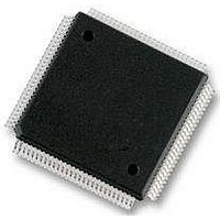
MC9S12E128CPV Freescale Semiconductor, MC9S12E128CPV Datasheet - Page 524

MC9S12E128CPV
Manufacturer Part Number
MC9S12E128CPV
Description
Microcontrollers (MCU) 16 Bit 16MHz
Manufacturer
Freescale Semiconductor
Datasheet
1.MC9S12E128CPV.pdf
(606 pages)
Specifications of MC9S12E128CPV
Data Bus Width
16 bit
Program Memory Type
Flash
Program Memory Size
128 KB
Data Ram Size
8 KB
Interface Type
SCI, SPI
Maximum Clock Frequency
25 MHz
Number Of Programmable I/os
92
Number Of Timers
16 bit
Operating Supply Voltage
3.135 V to 5.5 V
Maximum Operating Temperature
+ 85 C
Mounting Style
SMD/SMT
Package / Case
LQFP-112
Minimum Operating Temperature
- 40 C
On-chip Adc
10 bit
On-chip Dac
8 bit, 2 Channel
Lead Free Status / Rohs Status
No RoHS Version Available
Available stocks
Company
Part Number
Manufacturer
Quantity
Price
Company:
Part Number:
MC9S12E128CPVE
Manufacturer:
Freescale Semiconductor
Quantity:
10 000
- Current page: 524 of 606
- Download datasheet (4Mb)
Chapter 18 Multiplexed External Bus Interface (MEBIV3)
18.3.2.6
Read: Anytime when register is in the map
Write: Anytime when register is in the map
Port E is associated with external bus control signals and interrupt inputs. These include mode select
(MODB/IPIPE1, MODA/IPIPE0), E clock, size (LSTRB/TAGLO), read/write (R/W), IRQ, and XIRQ.
When not used for one of these specific functions, port E pins 7:2 can be used as general-purpose I/O and
pins 1:0 can be used as general-purpose input. The port E assignment register (PEAR) selects the function
of each pin and DDRE determines whether each pin is an input or output when it is configured to be
general-purpose I/O. DDRE also determines the source of data for a read of PORTE.
Some of these pins have software selectable pull resistors. IRQ and XIRQ can only be pulled up whereas
the polarity of the PE7, PE4, PE3, and PE2 pull resistors are determined by chip integration. Please refer
to the device overview chapter (Signal Property Summary) to determine the polarity of these resistors.
A single control bit enables the pull devices for all of these pins when they are configured as inputs.
This register is not in the on-chip map in special peripheral mode or in expanded modes when the EME
bit is set. Therefore, these accesses will be echoed externally.
524
Pin Function
Alternate
Reset
W
R
Port E Data Register (PORTE)
NOACC
It is unwise to write PORTE and DDRE as a word access. If you are
changing port E pins from being inputs to outputs, the data may have extra
transitions during the write. It is best to initialize PORTE before enabling as
outputs.
To ensure that you read the value present on the PORTE pins, always wait
at least one cycle after writing to the DDRE register before reading from the
PORTE register.
Bit 7
0
7
= Unimplemented or Reserved
or CLKTO
or IPIPE1
MODB
6
0
6
Figure 18-10. Port E Data Register (PORTE)
or IPIPE0
MC9S12E128 Data Sheet, Rev. 1.07
MODA
5
0
5
NOTE
NOTE
ECLK
4
0
4
u = Unaffected by reset
or TAGLO
LSTRB
3
3
0
R/W
2
2
0
Freescale Semiconductor
Bit 1
IRQ
u
1
XIRQ
Bit 0
u
0
Related parts for MC9S12E128CPV
Image
Part Number
Description
Manufacturer
Datasheet
Request
R
Part Number:
Description:
Manufacturer:
Freescale Semiconductor, Inc
Datasheet:
Part Number:
Description:
Manufacturer:
Freescale Semiconductor, Inc
Datasheet:
Part Number:
Description:
Manufacturer:
Freescale Semiconductor, Inc
Datasheet:
Part Number:
Description:
Manufacturer:
Freescale Semiconductor, Inc
Datasheet:
Part Number:
Description:
Manufacturer:
Freescale Semiconductor, Inc
Datasheet:
Part Number:
Description:
Manufacturer:
Freescale Semiconductor, Inc
Datasheet:
Part Number:
Description:
Manufacturer:
Freescale Semiconductor, Inc
Datasheet:
Part Number:
Description:
Manufacturer:
Freescale Semiconductor, Inc
Datasheet:
Part Number:
Description:
Manufacturer:
Freescale Semiconductor, Inc
Datasheet:
Part Number:
Description:
Manufacturer:
Freescale Semiconductor, Inc
Datasheet:
Part Number:
Description:
Manufacturer:
Freescale Semiconductor, Inc
Datasheet:
Part Number:
Description:
Manufacturer:
Freescale Semiconductor, Inc
Datasheet:
Part Number:
Description:
Manufacturer:
Freescale Semiconductor, Inc
Datasheet:
Part Number:
Description:
Manufacturer:
Freescale Semiconductor, Inc
Datasheet:
Part Number:
Description:
Manufacturer:
Freescale Semiconductor, Inc
Datasheet:


