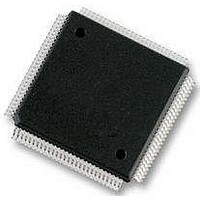
MC9S12E128CPV Freescale Semiconductor, MC9S12E128CPV Datasheet - Page 501

MC9S12E128CPV
Manufacturer Part Number
MC9S12E128CPV
Description
Microcontrollers (MCU) 16 Bit 16MHz
Manufacturer
Freescale Semiconductor
Datasheet
1.MC9S12E128CPV.pdf
(606 pages)
Specifications of MC9S12E128CPV
Data Bus Width
16 bit
Program Memory Type
Flash
Program Memory Size
128 KB
Data Ram Size
8 KB
Interface Type
SCI, SPI
Maximum Clock Frequency
25 MHz
Number Of Programmable I/os
92
Number Of Timers
16 bit
Operating Supply Voltage
3.135 V to 5.5 V
Maximum Operating Temperature
+ 85 C
Mounting Style
SMD/SMT
Package / Case
LQFP-112
Minimum Operating Temperature
- 40 C
On-chip Adc
10 bit
On-chip Dac
8 bit, 2 Channel
Lead Free Status / Rohs Status
No RoHS Version Available
Available stocks
Company
Part Number
Manufacturer
Quantity
Price
Company:
Part Number:
MC9S12E128CPVE
Manufacturer:
Freescale Semiconductor
Quantity:
10 000
- Current page: 501 of 606
- Download datasheet (4Mb)
16.4.2.6.3
In the detail mode, address and data for all cycles except program fetch (P) and free (f) cycles are stored
in trace buffer. This mode is intended to supply additional information on indexed, indirect addressing
modes where storing only the destination address would not provide all information required for a user to
determine where his code was in error.
16.4.2.6.4
This mode is intended to allow a host computer to poll a running target and provide a histogram of program
execution. Each read of the trace buffer address will return the address of the last instruction executed. The
DBGCNT register is not incremented and the trace buffer does not get filled. The ARM bit is not used and
all breakpoints and all other debug functions will be disabled.
16.4.2.7
The storage memory is a 64 words deep by 16-bits wide dual port RAM array. The CPU accesses the RAM
array through a single memory location window (DBGTBH:DBGTBL). The DBG module stores trace
information in the RAM array in a circular buffer format. As data is read via the CPU, a pointer into the
RAM will increment so that the next CPU read will receive fresh information. In all trigger modes except
for event-only and detail capture mode, the data stored in the trace buffer will be change-of-flow addresses.
change-of-flow addresses are defined as follows:
In the event-only trigger modes only the 16-bit data bus value corresponding to the event is stored. In the
detail capture mode, address and then data are stored for all cycles except program fetch (P) and free (f)
cycles.
16.4.2.8
16.4.2.8.1
Storing with begin-trigger can be used in all trigger modes. When DBG mode is enabled and armed in the
begin-trigger mode, data is not stored in the trace buffer until the trigger condition is met. As soon as the
trigger condition is met, the DBG module will remain armed until 64 words are stored in the trace buffer.
If the trigger is at the address of the change-of-flow instruction the change-of-flow associated with the
trigger event will be stored in the trace buffer.
16.4.2.8.2
Storing with end-trigger cannot be used in event-only trigger modes. When DBG mode is enabled and
armed in the end-trigger mode, data is stored in the trace buffer until the trigger condition is met. When
the trigger condition is met, the DBG module will become de-armed and no more data will be stored. If
Freescale Semiconductor
•
•
•
•
Source address of conditional branches (long, short, BRSET, and loop constructs) taken
Destination address of indexed JMP, JSR, and CALL instruction
Destination address of RTI, RTS, and RTC instructions
Vector address of interrupts except for SWI and BDM vectors
Storage Memory
Storing Data in Memory Storage Buffer
Detail Mode
Profile Mode
Storing with Begin-Trigger
Storing with End-Trigger
MC9S12E128 Data Sheet, Rev. 1.07
Chapter 16 Debug Module (DBGV1)
501
Related parts for MC9S12E128CPV
Image
Part Number
Description
Manufacturer
Datasheet
Request
R
Part Number:
Description:
Manufacturer:
Freescale Semiconductor, Inc
Datasheet:
Part Number:
Description:
Manufacturer:
Freescale Semiconductor, Inc
Datasheet:
Part Number:
Description:
Manufacturer:
Freescale Semiconductor, Inc
Datasheet:
Part Number:
Description:
Manufacturer:
Freescale Semiconductor, Inc
Datasheet:
Part Number:
Description:
Manufacturer:
Freescale Semiconductor, Inc
Datasheet:
Part Number:
Description:
Manufacturer:
Freescale Semiconductor, Inc
Datasheet:
Part Number:
Description:
Manufacturer:
Freescale Semiconductor, Inc
Datasheet:
Part Number:
Description:
Manufacturer:
Freescale Semiconductor, Inc
Datasheet:
Part Number:
Description:
Manufacturer:
Freescale Semiconductor, Inc
Datasheet:
Part Number:
Description:
Manufacturer:
Freescale Semiconductor, Inc
Datasheet:
Part Number:
Description:
Manufacturer:
Freescale Semiconductor, Inc
Datasheet:
Part Number:
Description:
Manufacturer:
Freescale Semiconductor, Inc
Datasheet:
Part Number:
Description:
Manufacturer:
Freescale Semiconductor, Inc
Datasheet:
Part Number:
Description:
Manufacturer:
Freescale Semiconductor, Inc
Datasheet:
Part Number:
Description:
Manufacturer:
Freescale Semiconductor, Inc
Datasheet:


