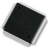
MC9S12E128CPV Freescale Semiconductor, MC9S12E128CPV Datasheet - Page 453

MC9S12E128CPV
Manufacturer Part Number
MC9S12E128CPV
Description
Microcontrollers (MCU) 16 Bit 16MHz
Manufacturer
Freescale Semiconductor
Datasheet
1.MC9S12E128CPV.pdf
(606 pages)
Specifications of MC9S12E128CPV
Data Bus Width
16 bit
Program Memory Type
Flash
Program Memory Size
128 KB
Data Ram Size
8 KB
Interface Type
SCI, SPI
Maximum Clock Frequency
25 MHz
Number Of Programmable I/os
92
Number Of Timers
16 bit
Operating Supply Voltage
3.135 V to 5.5 V
Maximum Operating Temperature
+ 85 C
Mounting Style
SMD/SMT
Package / Case
LQFP-112
Minimum Operating Temperature
- 40 C
On-chip Adc
10 bit
On-chip Dac
8 bit, 2 Channel
Lead Free Status / Rohs Status
No RoHS Version Available
Available stocks
Company
Part Number
Manufacturer
Quantity
Price
Company:
Part Number:
MC9S12E128CPVE
Manufacturer:
Freescale Semiconductor
Quantity:
10 000
- Current page: 453 of 606
- Download datasheet (4Mb)
Freescale Semiconductor
CLKSW
UNSEC
ENTAG
TRACE
Field
SDV
PLLSEL
5
4
3
2
1
0
0
Tagging Enable — This bit indicates whether instruction tagging in enabled or disabled. It is set when the
TAGGO command is executed and cleared when BDM is entered. The serial system is disabled and the tag
function enabled 16 cycles after this bit is written. BDM cannot process serial commands while tagging is active.
0 Tagging not enabled or BDM active
1 Tagging enabled
Shift Data Valid — This bit is set and cleared by the BDM hardware. It is set after data has been transmitted as
part of a firmware read command or after data has been received as part of a firmware write command. It is
cleared when the next BDM command has been received or BDM is exited. SDV is used by the standard BDM
firmware to control program flow execution.
0 Data phase of command not complete
1 Data phase of command is complete
TRACE1 BDM Firmware Command is Being Executed — This bit gets set when a BDM TRACE1 firmware
command is first recognized. It will stay set as long as continuous back-to-back TRACE1 commands are
executed. This bit will get cleared when the next command that is not a TRACE1 command is recognized.
0 TRACE1 command is not being executed
1 TRACE1 command is being executed
Clock Switch — The CLKSW bit controls which clock the BDM operates with. It is only writable from a hardware
BDM command. A 150 cycle delay at the clock speed that is active during the data portion of the command will
occur before the new clock source is guaranteed to be active. The start of the next BDM command uses the new
clock for timing subsequent BDM communications.
Table 15-3
clock and reset generator) bits.
Note: The BDM alternate clock source can only be selected when CLKSW = 0 and PLLSEL = 1. The BDM serial
Note: If the acknowledge function is turned on, changing the CLKSW bit will cause the ACK to be at the new rate
Unsecure — This bit is only writable in special single-chip mode from the BDM secure firmware and always gets
reset to zero. It is in a zero state as secure mode is entered so that the secure BDM firmware lookup table is
enabled and put into the memory map along with the standard BDM firmware lookup table.
The secure BDM firmware lookup table verifies that the on-chip EEPROM and FLASH EEPROM are erased. This
being the case, the UNSEC bit is set and the BDM program jumps to the start of the standard BDM firmware
lookup table and the secure BDM firmware lookup table is turned off. If the erase test fails, the UNSEC bit will
not be asserted.
0 System is in a secured mode
1 System is in a unsecured mode
Note: When UNSEC is set, security is off and the user can change the state of the secure bits in the on-chip
interface is now fully synchronized to the alternate clock source, when enabled. This eliminates frequency
restriction on the alternate clock which was required on previous versions. Refer to the device overview
section to determine which clock connects to the alternate clock source input.
for the write command which changes it.
FLASH EEPROM. Note that if the user does not change the state of the bits to “unsecured” mode, the
system will be secured again when it is next taken out of reset.
CLKSW
shows the resulting BDM clock source based on the CLKSW and the PLLSEL (Pll select from the
0
1
Table 15-2. BDMSTS Field Descriptions (continued)
Bus clock
Bus clock
Table 15-3. BDM Clock Sources
MC9S12E128 Data Sheet, Rev. 1.07
Description
BDMCLK
Chapter 15 Background Debug Module (BDMV4)
453
Related parts for MC9S12E128CPV
Image
Part Number
Description
Manufacturer
Datasheet
Request
R
Part Number:
Description:
Manufacturer:
Freescale Semiconductor, Inc
Datasheet:
Part Number:
Description:
Manufacturer:
Freescale Semiconductor, Inc
Datasheet:
Part Number:
Description:
Manufacturer:
Freescale Semiconductor, Inc
Datasheet:
Part Number:
Description:
Manufacturer:
Freescale Semiconductor, Inc
Datasheet:
Part Number:
Description:
Manufacturer:
Freescale Semiconductor, Inc
Datasheet:
Part Number:
Description:
Manufacturer:
Freescale Semiconductor, Inc
Datasheet:
Part Number:
Description:
Manufacturer:
Freescale Semiconductor, Inc
Datasheet:
Part Number:
Description:
Manufacturer:
Freescale Semiconductor, Inc
Datasheet:
Part Number:
Description:
Manufacturer:
Freescale Semiconductor, Inc
Datasheet:
Part Number:
Description:
Manufacturer:
Freescale Semiconductor, Inc
Datasheet:
Part Number:
Description:
Manufacturer:
Freescale Semiconductor, Inc
Datasheet:
Part Number:
Description:
Manufacturer:
Freescale Semiconductor, Inc
Datasheet:
Part Number:
Description:
Manufacturer:
Freescale Semiconductor, Inc
Datasheet:
Part Number:
Description:
Manufacturer:
Freescale Semiconductor, Inc
Datasheet:
Part Number:
Description:
Manufacturer:
Freescale Semiconductor, Inc
Datasheet:


