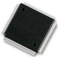
MC9S12E128CPV Freescale Semiconductor, MC9S12E128CPV Datasheet - Page 364

MC9S12E128CPV
Manufacturer Part Number
MC9S12E128CPV
Description
Microcontrollers (MCU) 16 Bit 16MHz
Manufacturer
Freescale Semiconductor
Datasheet
1.MC9S12E128CPV.pdf
(606 pages)
Specifications of MC9S12E128CPV
Data Bus Width
16 bit
Program Memory Type
Flash
Program Memory Size
128 KB
Data Ram Size
8 KB
Interface Type
SCI, SPI
Maximum Clock Frequency
25 MHz
Number Of Programmable I/os
92
Number Of Timers
16 bit
Operating Supply Voltage
3.135 V to 5.5 V
Maximum Operating Temperature
+ 85 C
Mounting Style
SMD/SMT
Package / Case
LQFP-112
Minimum Operating Temperature
- 40 C
On-chip Adc
10 bit
On-chip Dac
8 bit, 2 Channel
Lead Free Status / Rohs Status
No RoHS Version Available
Available stocks
Company
Part Number
Manufacturer
Quantity
Price
Company:
Part Number:
MC9S12E128CPVE
Manufacturer:
Freescale Semiconductor
Quantity:
10 000
- Current page: 364 of 606
- Download datasheet (4Mb)
Chapter 11 Pulse Width Modulator with Fault Protection (PMF15B6CV2)
11.4.5.1
In complementary mode, either the top or the bottom transistor controls the output voltage. However,
deadtime has to be inserted to avoid overlap of conducting interval between the top and bottom transistor.
Both transistors in complementary mode are off during deadtime, allowing the output voltage to be
determined by the current status of load and introduce distortion in the output voltage. See
On AC induction motors running open-loop, the distortion typically manifests itself as poor low-speed
performance, such as torque ripple and rough operation.
During deadtime, load inductance distorts output voltage by keeping current flowing through the diodes.
This deadtime current flow creates a load voltage that varies with current direction. With a positive current
flow, the load voltage during deadtime is equal to the bottom supply, putting the top transistor in control.
With a negative current flow, the load voltage during deadtime is equal to the top supply putting the bottom
transistor in control.
Remembering that the original PWM pulse widths were shortened by deadtime insertion, the averaged
sinusoidal output will be less than desired value. However, when deadtime is inserted, it creates a distortion
in motor current waveform. This distortion is aggravated by dissimilar turn-on and turn-off delays of each
of the transistors. By giving the PWM module information on which transistor is controlling at a given
time this distortion can be corrected.
For a typical circuit in complementary channel operation, only one of the transistors will be effective in
controlling the output voltage at any given time. This depends on the direction of the motor current for that
pair. See
value, depending on whether the top or bottom transistor is controlling the output voltage. Therefore, the
software is responsible for calculating both compensated PWM values prior to placing them in an
odd-numbered/even numbered PWM register pair. Either the odd or the even PMFVAL register controls
the pulse width at any given time.
364
Figure
Top/Bottom Correction
NEGATIVE CURRENT
POSITIVE CURRENT
11-53. To correct distortion one of two different factors must be added to the desired PWM
PWM TO BOTTOM
LOAD VOLTAGE
LOAD VOLTAGE
LOAD VOLTAGE
PWM TO TOP
TRANSISTOR
TRANSISTOR
DEADTIME
DESIRED
Figure 11-53. Deadtime Distortion
MC9S12E128 Data Sheet, Rev. 1.07
V+
CURRENT
NEGATIVE
CURRENT
POSITIVE
Freescale Semiconductor
Figure
11-53.
Related parts for MC9S12E128CPV
Image
Part Number
Description
Manufacturer
Datasheet
Request
R
Part Number:
Description:
Manufacturer:
Freescale Semiconductor, Inc
Datasheet:
Part Number:
Description:
Manufacturer:
Freescale Semiconductor, Inc
Datasheet:
Part Number:
Description:
Manufacturer:
Freescale Semiconductor, Inc
Datasheet:
Part Number:
Description:
Manufacturer:
Freescale Semiconductor, Inc
Datasheet:
Part Number:
Description:
Manufacturer:
Freescale Semiconductor, Inc
Datasheet:
Part Number:
Description:
Manufacturer:
Freescale Semiconductor, Inc
Datasheet:
Part Number:
Description:
Manufacturer:
Freescale Semiconductor, Inc
Datasheet:
Part Number:
Description:
Manufacturer:
Freescale Semiconductor, Inc
Datasheet:
Part Number:
Description:
Manufacturer:
Freescale Semiconductor, Inc
Datasheet:
Part Number:
Description:
Manufacturer:
Freescale Semiconductor, Inc
Datasheet:
Part Number:
Description:
Manufacturer:
Freescale Semiconductor, Inc
Datasheet:
Part Number:
Description:
Manufacturer:
Freescale Semiconductor, Inc
Datasheet:
Part Number:
Description:
Manufacturer:
Freescale Semiconductor, Inc
Datasheet:
Part Number:
Description:
Manufacturer:
Freescale Semiconductor, Inc
Datasheet:
Part Number:
Description:
Manufacturer:
Freescale Semiconductor, Inc
Datasheet:


