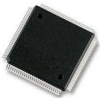
MC9S12E128CPV Freescale Semiconductor, MC9S12E128CPV Datasheet - Page 239

MC9S12E128CPV
Manufacturer Part Number
MC9S12E128CPV
Description
Microcontrollers (MCU) 16 Bit 16MHz
Manufacturer
Freescale Semiconductor
Datasheet
1.MC9S12E128CPV.pdf
(606 pages)
Specifications of MC9S12E128CPV
Data Bus Width
16 bit
Program Memory Type
Flash
Program Memory Size
128 KB
Data Ram Size
8 KB
Interface Type
SCI, SPI
Maximum Clock Frequency
25 MHz
Number Of Programmable I/os
92
Number Of Timers
16 bit
Operating Supply Voltage
3.135 V to 5.5 V
Maximum Operating Temperature
+ 85 C
Mounting Style
SMD/SMT
Package / Case
LQFP-112
Minimum Operating Temperature
- 40 C
On-chip Adc
10 bit
On-chip Dac
8 bit, 2 Channel
Lead Free Status / Rohs Status
No RoHS Version Available
Available stocks
Company
Part Number
Manufacturer
Quantity
Price
Company:
Part Number:
MC9S12E128CPVE
Manufacturer:
Freescale Semiconductor
Quantity:
10 000
- Current page: 239 of 606
- Download datasheet (4Mb)
7.2.1
This pin is used as the analog output pin of the DAC8B1C module. The value represents the analog voltage
level between V
7.2.2
This pin serves as the power supply pin.l
7.2.3
This pin serves as an analog ground reference to the DAC.
7.2.4
This pin serves as the source for the high reference potential. Separation from the power supply pins
accommodates the filtering necessary to achieve the accuracy of which the system is capable.
7.2.5
This pin serves as the ground for the low reference potential. This pin is connected to V
DAC module boundary to accommodate the filtering necessary to achieve the accuracy of which the
system is capable.
7.3
This section provides a detailed description of all memory and registers accessible to the end user.
7.3.1
Figure 7-2
address offset is defined at the module level.
Freescale Semiconductor
Address
0x0000
0x0001
0x0002
0x0003
Memory Map and Registers
DACD (Right
summarizes the DAC8B1C memory map. The base address is defined at the chip level and the
DACD (Left
DAO — DAC Channel Output
V
V
V
V
Module Memory Map
Justified)
Justified)
DACC0
DACC1
Name
DDA
SSA
REF
RL
SSA
— DAC Reference Ground Supply
— DAC Reference Supply
— DAC Ground Supply
— DAC Power Supply
and V
W
W
W
W
R
R
R
R
REF
DACE
BIT 7
BIT 7
Bit 7
.
0
Figure 7-2. DAC8B1C Register Summary
MC9S12E128 Data Sheet, Rev. 1.07
= Unimplemented or Reserved
DACTE
BIT 6
BIT 6
6
0
BIT 5
BIT 5
5
0
0
BIT 4
BIT 4
4
0
0
Chapter 7 Digital-to-Analog Converter (DAC8B1CV1)
BIT 3
BIT 3
DJM
3
0
DSGN
BIT 2
BIT 2
2
0
DACWAI
SSA
BIT 1
BIT 1
1
0
outside the
DACOE
BIT 0
BIT 0
Bit 0
0
239
Related parts for MC9S12E128CPV
Image
Part Number
Description
Manufacturer
Datasheet
Request
R
Part Number:
Description:
Manufacturer:
Freescale Semiconductor, Inc
Datasheet:
Part Number:
Description:
Manufacturer:
Freescale Semiconductor, Inc
Datasheet:
Part Number:
Description:
Manufacturer:
Freescale Semiconductor, Inc
Datasheet:
Part Number:
Description:
Manufacturer:
Freescale Semiconductor, Inc
Datasheet:
Part Number:
Description:
Manufacturer:
Freescale Semiconductor, Inc
Datasheet:
Part Number:
Description:
Manufacturer:
Freescale Semiconductor, Inc
Datasheet:
Part Number:
Description:
Manufacturer:
Freescale Semiconductor, Inc
Datasheet:
Part Number:
Description:
Manufacturer:
Freescale Semiconductor, Inc
Datasheet:
Part Number:
Description:
Manufacturer:
Freescale Semiconductor, Inc
Datasheet:
Part Number:
Description:
Manufacturer:
Freescale Semiconductor, Inc
Datasheet:
Part Number:
Description:
Manufacturer:
Freescale Semiconductor, Inc
Datasheet:
Part Number:
Description:
Manufacturer:
Freescale Semiconductor, Inc
Datasheet:
Part Number:
Description:
Manufacturer:
Freescale Semiconductor, Inc
Datasheet:
Part Number:
Description:
Manufacturer:
Freescale Semiconductor, Inc
Datasheet:
Part Number:
Description:
Manufacturer:
Freescale Semiconductor, Inc
Datasheet:


