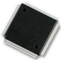
MC9S12E128CPV Freescale Semiconductor, MC9S12E128CPV Datasheet - Page 589

MC9S12E128CPV
Manufacturer Part Number
MC9S12E128CPV
Description
Microcontrollers (MCU) 16 Bit 16MHz
Manufacturer
Freescale Semiconductor
Datasheet
1.MC9S12E128CPV.pdf
(606 pages)
Specifications of MC9S12E128CPV
Data Bus Width
16 bit
Program Memory Type
Flash
Program Memory Size
128 KB
Data Ram Size
8 KB
Interface Type
SCI, SPI
Maximum Clock Frequency
25 MHz
Number Of Programmable I/os
92
Number Of Timers
16 bit
Operating Supply Voltage
3.135 V to 5.5 V
Maximum Operating Temperature
+ 85 C
Mounting Style
SMD/SMT
Package / Case
LQFP-112
Minimum Operating Temperature
- 40 C
On-chip Adc
10 bit
On-chip Dac
8 bit, 2 Channel
Lead Free Status / Rohs Status
No RoHS Version Available
Available stocks
Company
Part Number
Manufacturer
Quantity
Price
Company:
Part Number:
MC9S12E128CPVE
Manufacturer:
Freescale Semiconductor
Quantity:
10 000
- Current page: 589 of 606
- Download datasheet (4Mb)
1
2
3
A.6
This section describes the characteristics of the analog to digital converter.
The ATD is specified and tested for both the 3.3V and 5V range. For ranges between 3.3V and 5V the ATD
accuracy is generally the same as in the 3.3V range but is not tested in this range in production test.
A.6.1
The
The following constraints exist to obtain full-scale, full range results:
VSSA VRL VIN VRH VDDA This constraint exists since the sample buffer amplifier can not
drive beyond the power supply levels that it ties to. If the input level goes outside of this range it will
effectively be clipped.
Freescale Semiconductor
Conditions are shown in
Num C
Full accuracy is not guaranteed when differential voltage is less than 4.75V
The minimum time assumes a final sample period of 2 ATD clocks cycles while the maximum time assumes a final sample
period of 16 ATD clocks.
Reduced accuracy see
1
2
3
4
5
6
7
Table A-19
D Reference Potential
C Differential Reference Voltage
D ATD Clock Frequency
D ATD 10-Bit Conversion Period
D ATD 8-Bit Conversion Period
D Stop Recovery Time (V
P Reference Supply current
ATD Characteristics
ATD Operating Characteristics — 5V Range
shows conditions under which the ATD operates.
Conv, Time at 4.0MHz
Conv, Time at 2.0MHz ATD Clock f
Conv, Time at 2.0MHz ATD Clock f
Table A-4
Table A-22
Rating
DDA
unless otherwise noted. Supply Voltage 5V-10% <= VDDA <=5V+10%
Table A-19. 5V ATD Operating Characteristics
and
= 5.0 Volts)
1
Table
3
ATD Clock f
MC9S12E128 Data Sheet, Rev. 1.07
A-23.
Clock Cycles
Clock Cycles
ATDCLK
ATDCLK
ATDCLK
High
Low
2
1
V
N
T
T
Symbol
N
f
T
RH
ATDCLK
CONV10
CONV10
CONV10
CONV8
CONV8
I
V
V
t
REF
SR
RH
–V
RL
RL
V
V
4.75
Min
DDA/2
0.5
3.5
14
12
—
—
SSA
7
6
Appendix A Electrical Characteristics
Typ
5.0
—
—
—
—
—
—
—
—
—
—
V
0.375
V
Max
5.25
DDA/2
2.0
DDA
28
14
26
13
20
7
Cycles
Cycles
MHz
Unit
mA
V
V
V
s
s
s
s
589
Related parts for MC9S12E128CPV
Image
Part Number
Description
Manufacturer
Datasheet
Request
R
Part Number:
Description:
Manufacturer:
Freescale Semiconductor, Inc
Datasheet:
Part Number:
Description:
Manufacturer:
Freescale Semiconductor, Inc
Datasheet:
Part Number:
Description:
Manufacturer:
Freescale Semiconductor, Inc
Datasheet:
Part Number:
Description:
Manufacturer:
Freescale Semiconductor, Inc
Datasheet:
Part Number:
Description:
Manufacturer:
Freescale Semiconductor, Inc
Datasheet:
Part Number:
Description:
Manufacturer:
Freescale Semiconductor, Inc
Datasheet:
Part Number:
Description:
Manufacturer:
Freescale Semiconductor, Inc
Datasheet:
Part Number:
Description:
Manufacturer:
Freescale Semiconductor, Inc
Datasheet:
Part Number:
Description:
Manufacturer:
Freescale Semiconductor, Inc
Datasheet:
Part Number:
Description:
Manufacturer:
Freescale Semiconductor, Inc
Datasheet:
Part Number:
Description:
Manufacturer:
Freescale Semiconductor, Inc
Datasheet:
Part Number:
Description:
Manufacturer:
Freescale Semiconductor, Inc
Datasheet:
Part Number:
Description:
Manufacturer:
Freescale Semiconductor, Inc
Datasheet:
Part Number:
Description:
Manufacturer:
Freescale Semiconductor, Inc
Datasheet:
Part Number:
Description:
Manufacturer:
Freescale Semiconductor, Inc
Datasheet:


