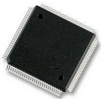
MC9S12E128CPV Freescale Semiconductor, MC9S12E128CPV Datasheet - Page 263

MC9S12E128CPV
Manufacturer Part Number
MC9S12E128CPV
Description
Microcontrollers (MCU) 16 Bit 16MHz
Manufacturer
Freescale Semiconductor
Datasheet
1.MC9S12E128CPV.pdf
(606 pages)
Specifications of MC9S12E128CPV
Data Bus Width
16 bit
Program Memory Type
Flash
Program Memory Size
128 KB
Data Ram Size
8 KB
Interface Type
SCI, SPI
Maximum Clock Frequency
25 MHz
Number Of Programmable I/os
92
Number Of Timers
16 bit
Operating Supply Voltage
3.135 V to 5.5 V
Maximum Operating Temperature
+ 85 C
Mounting Style
SMD/SMT
Package / Case
LQFP-112
Minimum Operating Temperature
- 40 C
On-chip Adc
10 bit
On-chip Dac
8 bit, 2 Channel
Lead Free Status / Rohs Status
No RoHS Version Available
Available stocks
Company
Part Number
Manufacturer
Quantity
Price
Company:
Part Number:
MC9S12E128CPVE
Manufacturer:
Freescale Semiconductor
Quantity:
10 000
- Current page: 263 of 606
- Download datasheet (4Mb)
flag by writing another byte to the transmitter buffer (SCIDRH/SCIDRL), while the shift register is
shifting out the first byte.
To initiate an SCI transmission:
Writing the TE bit from 0 to a 1 automatically loads the transmit shift register with a preamble of 10
logic 1s (if M = 0) or 11 logic 1s (if M = 1). After the preamble shifts out, control logic transfers the data
from the SCI data register into the transmit shift register. A logic 0 start bit automatically goes into the
least significant bit position of the transmit shift register. A logic 1 stop bit goes into the most significant
bit position.
Hardware supports odd or even parity. When parity is enabled, the most significant bit (MSB) of the data
character is the parity bit.
The transmit data register empty flag, TDRE, in SCI status register 1 (SCISR1) becomes set when the SCI
data register transfers a byte to the transmit shift register. The TDRE flag indicates that the SCI data
register can accept new data from the internal data bus. If the transmit interrupt enable bit, TIE, in SCI
control register 2 (SCICR2) is also set, the TDRE flag generates a transmitter interrupt request.
When the transmit shift register is not transmitting a frame, the TXD pin goes to the idle condition, logic 1.
If at any time software clears the TE bit in SCI control register 2 (SCICR2), the transmitter enable signal
goes low and the transmit signal goes idle.
Freescale Semiconductor
1. Configure the SCI:
2. Transmit procedure for each byte:
3. Repeat step 2 for each subsequent transmission.
a) Select a baud rate. Write this value to the SCI baud registers (SCIBDH/L) to begin the baud
b) Write to SCICR1 to configure word length, parity, and other configuration bits (LOOPS,
c) Enable the transmitter, interrupts, receive, and wake up as required, by writing to the SCICR2
a) Poll the TDRE flag by reading the SCISR1 or responding to the TDRE interrupt. Keep in mind
b) If the TDRE flag is set, write the data to be transmitted to SCIDRH/L, where the ninth bit is
rate generator. Remember that the baud rate generator is disabled when the baud rate is 0.
Writing to the SCIBDH has no effect without also writing to SCIBDL.
RSRC, M, WAKE, ILT, PE, and PT).
register bits (TIE, TCIE, RIE, ILIE, TE, RE, RWU, and SBK). A preamble or idle character
will now be shifted out of the transmitter shift register.
that the TDRE bit resets to 1.
written to the T8 bit in SCIDRH if the SCI is in 9-bit data format. A new transmission will not
result until the TDRE flag has been cleared.
The TDRE flag is set when the shift register is loaded with the next data to
be transmitted from SCIDRH/L, which happens, generally speaking, a little
over half-way through the stop bit of the previous frame. Specifically, this
transfer occurs 9/16ths of a bit time AFTER the start of the stop bit of the
previous frame.
MC9S12E128 Data Sheet, Rev. 1.07
NOTE
Chapter 8 Serial Communication Interface (SCIV3)
263
Related parts for MC9S12E128CPV
Image
Part Number
Description
Manufacturer
Datasheet
Request
R
Part Number:
Description:
Manufacturer:
Freescale Semiconductor, Inc
Datasheet:
Part Number:
Description:
Manufacturer:
Freescale Semiconductor, Inc
Datasheet:
Part Number:
Description:
Manufacturer:
Freescale Semiconductor, Inc
Datasheet:
Part Number:
Description:
Manufacturer:
Freescale Semiconductor, Inc
Datasheet:
Part Number:
Description:
Manufacturer:
Freescale Semiconductor, Inc
Datasheet:
Part Number:
Description:
Manufacturer:
Freescale Semiconductor, Inc
Datasheet:
Part Number:
Description:
Manufacturer:
Freescale Semiconductor, Inc
Datasheet:
Part Number:
Description:
Manufacturer:
Freescale Semiconductor, Inc
Datasheet:
Part Number:
Description:
Manufacturer:
Freescale Semiconductor, Inc
Datasheet:
Part Number:
Description:
Manufacturer:
Freescale Semiconductor, Inc
Datasheet:
Part Number:
Description:
Manufacturer:
Freescale Semiconductor, Inc
Datasheet:
Part Number:
Description:
Manufacturer:
Freescale Semiconductor, Inc
Datasheet:
Part Number:
Description:
Manufacturer:
Freescale Semiconductor, Inc
Datasheet:
Part Number:
Description:
Manufacturer:
Freescale Semiconductor, Inc
Datasheet:
Part Number:
Description:
Manufacturer:
Freescale Semiconductor, Inc
Datasheet:


