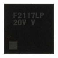
DF2117VLP20V Renesas Electronics America, DF2117VLP20V Datasheet - Page 17

DF2117VLP20V
Manufacturer Part Number
DF2117VLP20V
Description
IC H8S/2117 MCU FLASH 145TFLGA
Manufacturer
Renesas Electronics America
Series
H8® H8S/2100r
Datasheet
1.DF2117VBG20V.pdf
(960 pages)
Specifications of DF2117VLP20V
Core Processor
H8S/2600
Core Size
16-Bit
Speed
20MHz
Connectivity
FIFO, I²C, LPC, SCI, SmartCard
Peripherals
POR, PWM, WDT
Number Of I /o
112
Program Memory Size
160KB (160K x 8)
Program Memory Type
FLASH
Ram Size
8K x 8
Voltage - Supply (vcc/vdd)
3 V ~ 3.6 V
Data Converters
A/D 16x10b
Oscillator Type
External
Operating Temperature
-20°C ~ 75°C
Package / Case
145-TFLGA
For Use With
HS0005KCU11H - EMULATOR E10A-USB H8S(X),SH2(A)3DK2166 - DEV EVAL KIT H8S/2166
Lead Free Status / RoHS Status
Lead free / RoHS Compliant
Eeprom Size
-
Available stocks
Company
Part Number
Manufacturer
Quantity
Price
Company:
Part Number:
DF2117VLP20V
Manufacturer:
Renesas
Quantity:
100
Part Number:
DF2117VLP20V
Manufacturer:
RENESAS/瑞萨
Quantity:
20 000
- Current page: 17 of 960
- Download datasheet (6Mb)
Item
17.4.5 Slave Receive Operation
Figure 17.15 Example of Slave
Receive Mode Operation Timing
(2) (MLS = 0)
18.3 Register Descriptions
Table 18.2 Register
Configuration
18.3.2 Keyboard Buffer Control
Register 2 (KBCR2)
18.3.6 Keyboard Buffer Transmit
Data Register (KBTR)
18.4.8 Operation during Data
Reception
Figure 18.13 Receive Timing and
KCLK
18.4.9 KCLK Fall Interrupt
Operation
Figure 18.14 Example of KCLK
Input Fall Interrupt Operation
Page Revision (See Manual for Details)
547
564
567
572
581
582
Figure amended
User processing
Table amended
Table amended
Table amended
Figure amended
KCLK
KD
KBF
KCLK for
other PS 2
Note amended
Note: * The KBF setting timing is the same as the
Channel
Channel 0
Channel 1
Channel 2
Channel 3
Bit
7 to 4
Bit
7
6
5
4
3
2
1
0
ICDRR
Bit Name
⎯
Bit Name
KBT7
KBT6
KBT5
KBT4
KBT3
KBT2
KBT1
KBT0
Data (n-2)
Register Name
Keyboard control register 2_0
Keyboard control register 2_1
Keyboard control register 2_2
Keyboard control register 2_3
timing of KBF setting and KCLK automatic I/O
inhibit bit generation in figure 18.11. When the
KBF bit is used as the KCLK input fall interrupt
flag, the automatic I/O inhibit function does not
operate.
[9] Set ACKB=1
[8] IRIC clear
Start bit
1
Initial
Value
All 1
Initial
Value
1
1
1
1
1
1
1
1
[10] ICDR read (Data (n-1))
R/W
R/W
R/W
R/W
R/W
R/W
R/W
R/W
R/W
R/W
R/W
0
2
Rev. 3.00 Sep. 28, 2009 Page xv of xliv
Data (n-1)
Description
Reserved
These bits are always read as 1. The initial value
should not be changed.
Description
Keyboard Buffer Transmit Data Register 7 to 0
Initialized to H'FF at reset.
1
Abbreviation R/W
KBCR2_0
KBCR2_1
KBCR2_2
KBCR2_3
8
[8] IRIC clear
7
9
R/W
R/W
R/W
R/W
Parity
Initial
Value
H'F0
H'F0
H'F0
H'F0
10
REJ09B0350-0300
[10] ICDR read
(Data (n))
Address
H'FEDB
H'FEDF
H'FEE3
H'FFE3
Stop bit
11
Automatic I/O inhibit
Data (n)
[12] IRIC clear
Data Bus
Width
8
8
8
8
Related parts for DF2117VLP20V
Image
Part Number
Description
Manufacturer
Datasheet
Request
R

Part Number:
Description:
KIT STARTER FOR M16C/29
Manufacturer:
Renesas Electronics America
Datasheet:

Part Number:
Description:
KIT STARTER FOR R8C/2D
Manufacturer:
Renesas Electronics America
Datasheet:

Part Number:
Description:
R0K33062P STARTER KIT
Manufacturer:
Renesas Electronics America
Datasheet:

Part Number:
Description:
KIT STARTER FOR R8C/23 E8A
Manufacturer:
Renesas Electronics America
Datasheet:

Part Number:
Description:
KIT STARTER FOR R8C/25
Manufacturer:
Renesas Electronics America
Datasheet:

Part Number:
Description:
KIT STARTER H8S2456 SHARPE DSPLY
Manufacturer:
Renesas Electronics America
Datasheet:

Part Number:
Description:
KIT STARTER FOR R8C38C
Manufacturer:
Renesas Electronics America
Datasheet:

Part Number:
Description:
KIT STARTER FOR R8C35C
Manufacturer:
Renesas Electronics America
Datasheet:

Part Number:
Description:
KIT STARTER FOR R8CL3AC+LCD APPS
Manufacturer:
Renesas Electronics America
Datasheet:

Part Number:
Description:
KIT STARTER FOR RX610
Manufacturer:
Renesas Electronics America
Datasheet:

Part Number:
Description:
KIT STARTER FOR R32C/118
Manufacturer:
Renesas Electronics America
Datasheet:

Part Number:
Description:
KIT DEV RSK-R8C/26-29
Manufacturer:
Renesas Electronics America
Datasheet:

Part Number:
Description:
KIT STARTER FOR SH7124
Manufacturer:
Renesas Electronics America
Datasheet:

Part Number:
Description:
KIT STARTER FOR H8SX/1622
Manufacturer:
Renesas Electronics America
Datasheet:

Part Number:
Description:
KIT DEV FOR SH7203
Manufacturer:
Renesas Electronics America
Datasheet:


