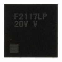
DF2117VLP20V Renesas Electronics America, DF2117VLP20V Datasheet - Page 49

DF2117VLP20V
Manufacturer Part Number
DF2117VLP20V
Description
IC H8S/2117 MCU FLASH 145TFLGA
Manufacturer
Renesas Electronics America
Series
H8® H8S/2100r
Datasheet
1.DF2117VBG20V.pdf
(960 pages)
Specifications of DF2117VLP20V
Core Processor
H8S/2600
Core Size
16-Bit
Speed
20MHz
Connectivity
FIFO, I²C, LPC, SCI, SmartCard
Peripherals
POR, PWM, WDT
Number Of I /o
112
Program Memory Size
160KB (160K x 8)
Program Memory Type
FLASH
Ram Size
8K x 8
Voltage - Supply (vcc/vdd)
3 V ~ 3.6 V
Data Converters
A/D 16x10b
Oscillator Type
External
Operating Temperature
-20°C ~ 75°C
Package / Case
145-TFLGA
For Use With
HS0005KCU11H - EMULATOR E10A-USB H8S(X),SH2(A)3DK2166 - DEV EVAL KIT H8S/2166
Lead Free Status / RoHS Status
Lead free / RoHS Compliant
Eeprom Size
-
Available stocks
Company
Part Number
Manufacturer
Quantity
Price
Company:
Part Number:
DF2117VLP20V
Manufacturer:
Renesas
Quantity:
100
Part Number:
DF2117VLP20V
Manufacturer:
RENESAS/瑞萨
Quantity:
20 000
- Current page: 49 of 960
- Download datasheet (6Mb)
Classification
CPU
Interrupt
(source)
Clock
A/D converter
Module/
Function
MCU
operating
mode
Interrupt
controller
Clock pulse
generator
(CPG)
A/D
converter
(ADC)
Description
Mode 2: Single-chip mode
Mode 4: Boot mode
Mode 6: On-chip emulation mode
Note: MD0 is not available as a pin and is internally fixed to 0.
•
•
•
•
•
•
•
•
•
•
•
•
•
•
Power-down state (transition to the power-down state made by
the SLEEP instruction)
41 external interrupt pins (NMI, IRQ15 to IRQ0 (ExIRQ15 to
ExIRQ6), KIN15 to KIN0, and WUE15 to WUE8)
63 internal interrupt sources
Two interrupt control modes (specified by the system control
register)
Two levels of interrupt priority orders specifiable (by setting the
interrupt control register)
Independent vector addresses
Two clock generation circuits
Clock pulse generator and subclock input circuit
System clock (φ) synchronization: 8 to 20 MHz
Five power-down modes: Medium-speed mode, sleep mode,
watch mode, software standby mode, and module stop mode
10-bit resolution × 16 input channels
Sample and hold function included
Conversion time: 4 μs per channel (with A/D conversion clock
ADCLK at 10 MHz operation)
Two operating modes: single mode and scan mode
Three methods to start A/D conversion: software and two timer
(TPU/TMR) triggers
(selected by driving the MD2 and MD0 pins low and MD1
pin high)
(selected by driving the MD2 high and MD1 and MD0 pins
low)
(selected by driving the MD2 and MD1 pins high and the
MD0 pin low)
Rev. 3.00 Sep. 28, 2009 Page 3 of 910
Section 1 Overview
REJ09B0350-0300
Related parts for DF2117VLP20V
Image
Part Number
Description
Manufacturer
Datasheet
Request
R

Part Number:
Description:
KIT STARTER FOR M16C/29
Manufacturer:
Renesas Electronics America
Datasheet:

Part Number:
Description:
KIT STARTER FOR R8C/2D
Manufacturer:
Renesas Electronics America
Datasheet:

Part Number:
Description:
R0K33062P STARTER KIT
Manufacturer:
Renesas Electronics America
Datasheet:

Part Number:
Description:
KIT STARTER FOR R8C/23 E8A
Manufacturer:
Renesas Electronics America
Datasheet:

Part Number:
Description:
KIT STARTER FOR R8C/25
Manufacturer:
Renesas Electronics America
Datasheet:

Part Number:
Description:
KIT STARTER H8S2456 SHARPE DSPLY
Manufacturer:
Renesas Electronics America
Datasheet:

Part Number:
Description:
KIT STARTER FOR R8C38C
Manufacturer:
Renesas Electronics America
Datasheet:

Part Number:
Description:
KIT STARTER FOR R8C35C
Manufacturer:
Renesas Electronics America
Datasheet:

Part Number:
Description:
KIT STARTER FOR R8CL3AC+LCD APPS
Manufacturer:
Renesas Electronics America
Datasheet:

Part Number:
Description:
KIT STARTER FOR RX610
Manufacturer:
Renesas Electronics America
Datasheet:

Part Number:
Description:
KIT STARTER FOR R32C/118
Manufacturer:
Renesas Electronics America
Datasheet:

Part Number:
Description:
KIT DEV RSK-R8C/26-29
Manufacturer:
Renesas Electronics America
Datasheet:

Part Number:
Description:
KIT STARTER FOR SH7124
Manufacturer:
Renesas Electronics America
Datasheet:

Part Number:
Description:
KIT STARTER FOR H8SX/1622
Manufacturer:
Renesas Electronics America
Datasheet:

Part Number:
Description:
KIT DEV FOR SH7203
Manufacturer:
Renesas Electronics America
Datasheet:


