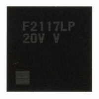
DF2117VLP20V Renesas Electronics America, DF2117VLP20V Datasheet - Page 616

DF2117VLP20V
Manufacturer Part Number
DF2117VLP20V
Description
IC H8S/2117 MCU FLASH 145TFLGA
Manufacturer
Renesas Electronics America
Series
H8® H8S/2100r
Datasheet
1.DF2117VBG20V.pdf
(960 pages)
Specifications of DF2117VLP20V
Core Processor
H8S/2600
Core Size
16-Bit
Speed
20MHz
Connectivity
FIFO, I²C, LPC, SCI, SmartCard
Peripherals
POR, PWM, WDT
Number Of I /o
112
Program Memory Size
160KB (160K x 8)
Program Memory Type
FLASH
Ram Size
8K x 8
Voltage - Supply (vcc/vdd)
3 V ~ 3.6 V
Data Converters
A/D 16x10b
Oscillator Type
External
Operating Temperature
-20°C ~ 75°C
Package / Case
145-TFLGA
For Use With
HS0005KCU11H - EMULATOR E10A-USB H8S(X),SH2(A)3DK2166 - DEV EVAL KIT H8S/2166
Lead Free Status / RoHS Status
Lead free / RoHS Compliant
Eeprom Size
-
Available stocks
Company
Part Number
Manufacturer
Quantity
Price
Company:
Part Number:
DF2117VLP20V
Manufacturer:
Renesas
Quantity:
100
Part Number:
DF2117VLP20V
Manufacturer:
RENESAS/瑞萨
Quantity:
20 000
- Current page: 616 of 960
- Download datasheet (6Mb)
Section 18 Keyboard Buffer Control Unit (PS2)
18.3.4
KBCRL enables the receive counter count and controls the keyboard buffer control unit pin
output.
Rev. 3.00 Sep. 28, 2009 Page 570 of 910
REJ09B0350-0300
Bit
7
6
5
4
Bit Name
KBE
KCLKO
KDO
—
Keyboard Control Register L (KBCRL)
Initial
Value
0
1
1
1
R/W
R/W
R/W
R/W
—
Description
Keyboard Enable
Enables or disables loading of receive data into KBBR.
0: Loading of receive data into KBBR is disabled
1: Loading of receive data into KBBR is enabled
Keyboard Clock Out
Controls PS2 clock I/O pin output.
0: PS2 clock I/O pin is low
1: PS2 clock I/O pin is high
Keyboard Data Out
Controls PS2 data I/O pin output.
0: PS2 data I/O pin is low
1: PS2 data I/O pin is high
When the start bit (KDO) is automatically cleared
(KDO = 1) by means of automatic transmission, 0 is
written after reading 1.
Reserved
This bit is always read as 1 and cannot be modified.
Related parts for DF2117VLP20V
Image
Part Number
Description
Manufacturer
Datasheet
Request
R

Part Number:
Description:
KIT STARTER FOR M16C/29
Manufacturer:
Renesas Electronics America
Datasheet:

Part Number:
Description:
KIT STARTER FOR R8C/2D
Manufacturer:
Renesas Electronics America
Datasheet:

Part Number:
Description:
R0K33062P STARTER KIT
Manufacturer:
Renesas Electronics America
Datasheet:

Part Number:
Description:
KIT STARTER FOR R8C/23 E8A
Manufacturer:
Renesas Electronics America
Datasheet:

Part Number:
Description:
KIT STARTER FOR R8C/25
Manufacturer:
Renesas Electronics America
Datasheet:

Part Number:
Description:
KIT STARTER H8S2456 SHARPE DSPLY
Manufacturer:
Renesas Electronics America
Datasheet:

Part Number:
Description:
KIT STARTER FOR R8C38C
Manufacturer:
Renesas Electronics America
Datasheet:

Part Number:
Description:
KIT STARTER FOR R8C35C
Manufacturer:
Renesas Electronics America
Datasheet:

Part Number:
Description:
KIT STARTER FOR R8CL3AC+LCD APPS
Manufacturer:
Renesas Electronics America
Datasheet:

Part Number:
Description:
KIT STARTER FOR RX610
Manufacturer:
Renesas Electronics America
Datasheet:

Part Number:
Description:
KIT STARTER FOR R32C/118
Manufacturer:
Renesas Electronics America
Datasheet:

Part Number:
Description:
KIT DEV RSK-R8C/26-29
Manufacturer:
Renesas Electronics America
Datasheet:

Part Number:
Description:
KIT STARTER FOR SH7124
Manufacturer:
Renesas Electronics America
Datasheet:

Part Number:
Description:
KIT STARTER FOR H8SX/1622
Manufacturer:
Renesas Electronics America
Datasheet:

Part Number:
Description:
KIT DEV FOR SH7203
Manufacturer:
Renesas Electronics America
Datasheet:


