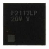
DF2117VLP20V Renesas Electronics America, DF2117VLP20V Datasheet - Page 562

DF2117VLP20V
Manufacturer Part Number
DF2117VLP20V
Description
IC H8S/2117 MCU FLASH 145TFLGA
Manufacturer
Renesas Electronics America
Series
H8® H8S/2100r
Datasheet
1.DF2117VBG20V.pdf
(960 pages)
Specifications of DF2117VLP20V
Core Processor
H8S/2600
Core Size
16-Bit
Speed
20MHz
Connectivity
FIFO, I²C, LPC, SCI, SmartCard
Peripherals
POR, PWM, WDT
Number Of I /o
112
Program Memory Size
160KB (160K x 8)
Program Memory Type
FLASH
Ram Size
8K x 8
Voltage - Supply (vcc/vdd)
3 V ~ 3.6 V
Data Converters
A/D 16x10b
Oscillator Type
External
Operating Temperature
-20°C ~ 75°C
Package / Case
145-TFLGA
For Use With
HS0005KCU11H - EMULATOR E10A-USB H8S(X),SH2(A)3DK2166 - DEV EVAL KIT H8S/2166
Lead Free Status / RoHS Status
Lead free / RoHS Compliant
Eeprom Size
-
Available stocks
Company
Part Number
Manufacturer
Quantity
Price
Company:
Part Number:
DF2117VLP20V
Manufacturer:
Renesas
Quantity:
100
Part Number:
DF2117VLP20V
Manufacturer:
RENESAS/瑞萨
Quantity:
20 000
- Current page: 562 of 960
- Download datasheet (6Mb)
Section 17 I
17.3.5
ICCR controls the I
Rev. 3.00 Sep. 28, 2009 Page 516 of 910
REJ09B0350-0300
Bit
7
6
5
4
Bit Name
ICE
IEIC
MST
TRS
I
2
C Bus Control Register (ICCR)
2
C Bus Interface (IIC)
2
C bus interface and performs interrupt flag confirmation.
Initial
Value
0
0
0
0
R/W
R/W
R/W
R/W
R/W
Description
I
0: I
1: I
I
0: Disables interrupts from the I
1: Enables interrupts from the I
Master/Slave Select
Transmit/Receive Select
MST TRS
Both these bits will be cleared by hardware when they
lose in a bus contention in master mode with the I
bus format. In slave receive mode with I
the R/W bit in the first frame immediately after the start
condition sets these bits in receive mode or transmit
mode automatically by hardware.
Modification of the TRS bit during transfer is deferred
until transfer is completed, and the changeover is made
after completion of the transfer (at the rising edge of
the 9th clock).
2
2
C Bus Interface Enable
C Bus Interface Interrupt Enable
0
0
1
1
interface module internal state is initialized. SAR
and SARX can be accessed.
operation, and the ports function as the SCL and
SDA input/output pins. ICMR and ICDR can be
accessed.
CPU
CPU.
2
2
C bus interface modules are stopped and I
C bus interface modules can perform transfer
0:
1:
0:
1:
Slave receive mode
Slave transmit mode
Master receive mode
Master transmit mode
2
2
C bus interface to the
C bus interface to the
2
C bus format,
2
C bus
2
C
Related parts for DF2117VLP20V
Image
Part Number
Description
Manufacturer
Datasheet
Request
R

Part Number:
Description:
KIT STARTER FOR M16C/29
Manufacturer:
Renesas Electronics America
Datasheet:

Part Number:
Description:
KIT STARTER FOR R8C/2D
Manufacturer:
Renesas Electronics America
Datasheet:

Part Number:
Description:
R0K33062P STARTER KIT
Manufacturer:
Renesas Electronics America
Datasheet:

Part Number:
Description:
KIT STARTER FOR R8C/23 E8A
Manufacturer:
Renesas Electronics America
Datasheet:

Part Number:
Description:
KIT STARTER FOR R8C/25
Manufacturer:
Renesas Electronics America
Datasheet:

Part Number:
Description:
KIT STARTER H8S2456 SHARPE DSPLY
Manufacturer:
Renesas Electronics America
Datasheet:

Part Number:
Description:
KIT STARTER FOR R8C38C
Manufacturer:
Renesas Electronics America
Datasheet:

Part Number:
Description:
KIT STARTER FOR R8C35C
Manufacturer:
Renesas Electronics America
Datasheet:

Part Number:
Description:
KIT STARTER FOR R8CL3AC+LCD APPS
Manufacturer:
Renesas Electronics America
Datasheet:

Part Number:
Description:
KIT STARTER FOR RX610
Manufacturer:
Renesas Electronics America
Datasheet:

Part Number:
Description:
KIT STARTER FOR R32C/118
Manufacturer:
Renesas Electronics America
Datasheet:

Part Number:
Description:
KIT DEV RSK-R8C/26-29
Manufacturer:
Renesas Electronics America
Datasheet:

Part Number:
Description:
KIT STARTER FOR SH7124
Manufacturer:
Renesas Electronics America
Datasheet:

Part Number:
Description:
KIT STARTER FOR H8SX/1622
Manufacturer:
Renesas Electronics America
Datasheet:

Part Number:
Description:
KIT DEV FOR SH7203
Manufacturer:
Renesas Electronics America
Datasheet:


