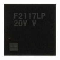
DF2117VLP20V Renesas Electronics America, DF2117VLP20V Datasheet - Page 658

DF2117VLP20V
Manufacturer Part Number
DF2117VLP20V
Description
IC H8S/2117 MCU FLASH 145TFLGA
Manufacturer
Renesas Electronics America
Series
H8® H8S/2100r
Datasheet
1.DF2117VBG20V.pdf
(960 pages)
Specifications of DF2117VLP20V
Core Processor
H8S/2600
Core Size
16-Bit
Speed
20MHz
Connectivity
FIFO, I²C, LPC, SCI, SmartCard
Peripherals
POR, PWM, WDT
Number Of I /o
112
Program Memory Size
160KB (160K x 8)
Program Memory Type
FLASH
Ram Size
8K x 8
Voltage - Supply (vcc/vdd)
3 V ~ 3.6 V
Data Converters
A/D 16x10b
Oscillator Type
External
Operating Temperature
-20°C ~ 75°C
Package / Case
145-TFLGA
For Use With
HS0005KCU11H - EMULATOR E10A-USB H8S(X),SH2(A)3DK2166 - DEV EVAL KIT H8S/2166
Lead Free Status / RoHS Status
Lead free / RoHS Compliant
Eeprom Size
-
Available stocks
Company
Part Number
Manufacturer
Quantity
Price
Company:
Part Number:
DF2117VLP20V
Manufacturer:
Renesas
Quantity:
100
Part Number:
DF2117VLP20V
Manufacturer:
RENESAS/瑞萨
Quantity:
20 000
- Current page: 658 of 960
- Download datasheet (6Mb)
Section 19 LPC Interface (LPC)
• Host select register
Note:
19.3.9
IDR1 to IDR4 are 8-bit read-only registers for the slave (this LSI), and 8-bit write-only registers
for the host. The registers selected from the host according to the I/O address are shown in the
following table. Data transferred in an LPC I/O write cycle is written to the selected register. The
value of bit 2 of the I/O address is latched into the C/D bit in STR, to indicate whether the written
information is a command or data. The initial values of IDR1 to IDR4 are H'00.
n = 1 to 4
19.3.10 Output Data Registers 1 to 4 (ODR1 to ODR4)
ODR1 to ODR4 are 8-bit readable/writable registers for the slave (this LSI), and 8-bit read-only
registers for the host. The registers selected from the host according to the I/O address are shown
in the following table. In an LPC I/O read cycle, the data in the selected register is transferred to
the host. The initial values of ODR1 to ODR4 are H'00.
n = 1 to 4
Rev. 3.00 Sep. 28, 2009 Page 612 of 910
REJ09B0350-0300
Bits 5 to 3
Bits 15 to 3 in LADR4
Bits 15 to 3 in LADR4
Bits 15 to 3 in LADR4
Bits 15 to 3 in LADR4
Bits 15 to 4
Bits 15 to 4
Bits 15 to 4
Bits 15 to 4
Bits 15 to 4
* When channel 4 is used, the content of LADR4 must be set so that the addresses for
Input Data Registers 1 to 4 (IDR1 to IDR4)
channels 1, 2, 3 and SCIF are different.
Bit 3
Bit 3
Bit 3
Bit 3
Bit 3
I/O Address
I/O Address
I/O Address
Bit 2
0
1
Bit 2
0
Bit 2
0
1
0
1
Bits 1 and 0
Bits 1 and 0 in LADR4
Bits 1 and 0 in LADR4
Bits 1 and 0 in LADR4
Bits 1 and 0 in LADR4
Bit 1
Bit 1
Bit 1
Bit 1
Bit1
Bit 0
Bit 0
Bit 0
Bit 0
Bit 0
I/O write
I/O write
Transfer
Cycle
Transfer
Cycle
I/O read
Transfer
Cycle
I/O write
I/O write
I/O read
I/O read
Host Register Selection
IDRn write, C/Dn ← 0
IDRn write, C/Dn ← 1
Host Register Selection
ODRn read
Host Select Register
IDR4 write (data)
IDR4 write (command)
ODR4 read
STR4 read
Related parts for DF2117VLP20V
Image
Part Number
Description
Manufacturer
Datasheet
Request
R

Part Number:
Description:
KIT STARTER FOR M16C/29
Manufacturer:
Renesas Electronics America
Datasheet:

Part Number:
Description:
KIT STARTER FOR R8C/2D
Manufacturer:
Renesas Electronics America
Datasheet:

Part Number:
Description:
R0K33062P STARTER KIT
Manufacturer:
Renesas Electronics America
Datasheet:

Part Number:
Description:
KIT STARTER FOR R8C/23 E8A
Manufacturer:
Renesas Electronics America
Datasheet:

Part Number:
Description:
KIT STARTER FOR R8C/25
Manufacturer:
Renesas Electronics America
Datasheet:

Part Number:
Description:
KIT STARTER H8S2456 SHARPE DSPLY
Manufacturer:
Renesas Electronics America
Datasheet:

Part Number:
Description:
KIT STARTER FOR R8C38C
Manufacturer:
Renesas Electronics America
Datasheet:

Part Number:
Description:
KIT STARTER FOR R8C35C
Manufacturer:
Renesas Electronics America
Datasheet:

Part Number:
Description:
KIT STARTER FOR R8CL3AC+LCD APPS
Manufacturer:
Renesas Electronics America
Datasheet:

Part Number:
Description:
KIT STARTER FOR RX610
Manufacturer:
Renesas Electronics America
Datasheet:

Part Number:
Description:
KIT STARTER FOR R32C/118
Manufacturer:
Renesas Electronics America
Datasheet:

Part Number:
Description:
KIT DEV RSK-R8C/26-29
Manufacturer:
Renesas Electronics America
Datasheet:

Part Number:
Description:
KIT STARTER FOR SH7124
Manufacturer:
Renesas Electronics America
Datasheet:

Part Number:
Description:
KIT STARTER FOR H8SX/1622
Manufacturer:
Renesas Electronics America
Datasheet:

Part Number:
Description:
KIT DEV FOR SH7203
Manufacturer:
Renesas Electronics America
Datasheet:


