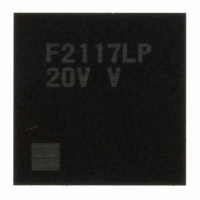
DF2117VLP20V Renesas Electronics America, DF2117VLP20V Datasheet - Page 592

DF2117VLP20V
Manufacturer Part Number
DF2117VLP20V
Description
IC H8S/2117 MCU FLASH 145TFLGA
Manufacturer
Renesas Electronics America
Series
H8® H8S/2100r
Datasheet
1.DF2117VBG20V.pdf
(960 pages)
Specifications of DF2117VLP20V
Core Processor
H8S/2600
Core Size
16-Bit
Speed
20MHz
Connectivity
FIFO, I²C, LPC, SCI, SmartCard
Peripherals
POR, PWM, WDT
Number Of I /o
112
Program Memory Size
160KB (160K x 8)
Program Memory Type
FLASH
Ram Size
8K x 8
Voltage - Supply (vcc/vdd)
3 V ~ 3.6 V
Data Converters
A/D 16x10b
Oscillator Type
External
Operating Temperature
-20°C ~ 75°C
Package / Case
145-TFLGA
For Use With
HS0005KCU11H - EMULATOR E10A-USB H8S(X),SH2(A)3DK2166 - DEV EVAL KIT H8S/2166
Lead Free Status / RoHS Status
Lead free / RoHS Compliant
Eeprom Size
-
Available stocks
Company
Part Number
Manufacturer
Quantity
Price
Company:
Part Number:
DF2117VLP20V
Manufacturer:
Renesas
Quantity:
100
Part Number:
DF2117VLP20V
Manufacturer:
RENESAS/瑞萨
Quantity:
20 000
- Current page: 592 of 960
- Download datasheet (6Mb)
Section 17 I
The slave mode reception procedure and operations are described below.
1. Initialize the IIC as described in section 17.4.2, Initialization.
2. Confirm that the ICDRF flag is 0. If the ICDRF flag is set to 1, read the ICDR and then clear
3. When the start condition output by the master device is detected, the BBSY flag in ICCR is set
4. When the slave address matches in the first frame following the start condition, the device
5. At the 9th clock pulse of the receive frame, the slave device returns the data in the ACKB bit
6. At the rise of the 9th clock pulse, the IRIC flag is set to 1. If the IEIC bit has been set to 1, an
7. At the rise of the 9th clock pulse, the receive data is transferred from ICDRS to ICDRR,
8. Confirm that the STOP bit is cleared to 0, and clear the IRIC flag to 0.
9. If the next frame is the last receive frame, set the ACKB bit to 1.
10. If ICDR is read, the ICDRF flag is cleared to 0, releasing the SCL bus line. This enables the
Receive operations can be performed continuously by repeating steps [5] to [10].
11. When the stop condition is detected (SDA is changed from low to high when SCL is high), the
12. Confirm that the STOP bit is set to 1, and clear the IRIC flag to 0.
Rev. 3.00 Sep. 28, 2009 Page 546 of 910
REJ09B0350-0300
Clear the MST and TRS bits to 0 to set slave receive mode, and set the ACKB bit to 0. Clear
the IRIC flag in ICCR to 0 to see the end of reception.
the IRIC flag to 0.
to 1. The master device then outputs the 7-bit slave address and transmit/receive direction
(R/W), in synchronization with the transmit clock pulses.
operates as the slave device specified by the master device. If the 8th data bit (R/W) is 0, the
TRS bit remains cleared to 0, and slave receive operation is performed. If the 8th data bit
(R/W) is 1, the TRS bit is set to 1, and slave transmit operation is performed. When the slave
address does not match, receive operation is halted until the next start condition is detected.
as an acknowledge signal.
interrupt request is sent to the CPU.
If the AASX bit has been set to 1, IRTR flag is also set to 1.
setting the ICDRF flag to 1. The slave device drives SCL low from the fall of the 9th receive
clock pulse until data is read from ICDR.
master device to transfer the next data.
BBSY flag is cleared to 0 and the STOP bit is set to 1. If the STOPIM bit has been cleared to
0, the IRIC flag is set to 1.
2
C Bus Interface (IIC)
Related parts for DF2117VLP20V
Image
Part Number
Description
Manufacturer
Datasheet
Request
R

Part Number:
Description:
KIT STARTER FOR M16C/29
Manufacturer:
Renesas Electronics America
Datasheet:

Part Number:
Description:
KIT STARTER FOR R8C/2D
Manufacturer:
Renesas Electronics America
Datasheet:

Part Number:
Description:
R0K33062P STARTER KIT
Manufacturer:
Renesas Electronics America
Datasheet:

Part Number:
Description:
KIT STARTER FOR R8C/23 E8A
Manufacturer:
Renesas Electronics America
Datasheet:

Part Number:
Description:
KIT STARTER FOR R8C/25
Manufacturer:
Renesas Electronics America
Datasheet:

Part Number:
Description:
KIT STARTER H8S2456 SHARPE DSPLY
Manufacturer:
Renesas Electronics America
Datasheet:

Part Number:
Description:
KIT STARTER FOR R8C38C
Manufacturer:
Renesas Electronics America
Datasheet:

Part Number:
Description:
KIT STARTER FOR R8C35C
Manufacturer:
Renesas Electronics America
Datasheet:

Part Number:
Description:
KIT STARTER FOR R8CL3AC+LCD APPS
Manufacturer:
Renesas Electronics America
Datasheet:

Part Number:
Description:
KIT STARTER FOR RX610
Manufacturer:
Renesas Electronics America
Datasheet:

Part Number:
Description:
KIT STARTER FOR R32C/118
Manufacturer:
Renesas Electronics America
Datasheet:

Part Number:
Description:
KIT DEV RSK-R8C/26-29
Manufacturer:
Renesas Electronics America
Datasheet:

Part Number:
Description:
KIT STARTER FOR SH7124
Manufacturer:
Renesas Electronics America
Datasheet:

Part Number:
Description:
KIT STARTER FOR H8SX/1622
Manufacturer:
Renesas Electronics America
Datasheet:

Part Number:
Description:
KIT DEV FOR SH7203
Manufacturer:
Renesas Electronics America
Datasheet:


