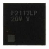
DF2117VLP20V Renesas Electronics America, DF2117VLP20V Datasheet - Page 69

DF2117VLP20V
Manufacturer Part Number
DF2117VLP20V
Description
IC H8S/2117 MCU FLASH 145TFLGA
Manufacturer
Renesas Electronics America
Series
H8® H8S/2100r
Datasheet
1.DF2117VBG20V.pdf
(960 pages)
Specifications of DF2117VLP20V
Core Processor
H8S/2600
Core Size
16-Bit
Speed
20MHz
Connectivity
FIFO, I²C, LPC, SCI, SmartCard
Peripherals
POR, PWM, WDT
Number Of I /o
112
Program Memory Size
160KB (160K x 8)
Program Memory Type
FLASH
Ram Size
8K x 8
Voltage - Supply (vcc/vdd)
3 V ~ 3.6 V
Data Converters
A/D 16x10b
Oscillator Type
External
Operating Temperature
-20°C ~ 75°C
Package / Case
145-TFLGA
For Use With
HS0005KCU11H - EMULATOR E10A-USB H8S(X),SH2(A)3DK2166 - DEV EVAL KIT H8S/2166
Lead Free Status / RoHS Status
Lead free / RoHS Compliant
Eeprom Size
-
Available stocks
Company
Part Number
Manufacturer
Quantity
Price
Company:
Part Number:
DF2117VLP20V
Manufacturer:
Renesas
Quantity:
100
Part Number:
DF2117VLP20V
Manufacturer:
RENESAS/瑞萨
Quantity:
20 000
- Current page: 69 of 960
- Download datasheet (6Mb)
Type
Serial
communic-
ation
interface
with FIFO
(SCIF)
LPC
Interface
(LPC)
Symbol
FTxD
FRxD
RI
DCD
DSR
DTR
CTS
RTS
LAD3 to
LAD0
LFRAME 125
LRESET
LCLK
SERIRQ
LSCI,
LSMI,
PME
GA20
CLKRUN 131
LPCPD
16
15
118
117
116
115
114
113
124 to
121
126
127
128
119, 120,
129
130
132
TFP-144V
B9, A9, C9,
D9
D8
C8
A8
D7
A10, B10,
C7
A7
B7
D6
G1
G4
D10
A11
B11
C11
A12
D11
BP-176V TLP-145V
Pin No.
G2
F3
B9
A10
B10
A11
A8
D8
B6
D5
C10
C11
B7, C8, D9,
A9
D7
D6
C9, B8, A7 Input/
C7
I/O
Output Transmit data output pin.
Input
Input
Input
Input
Output Data terminal ready output
Input
Output Transmission request output
Input/
Output
Input
Input
Input
Input/
Output
Output
Input/
Output
Input/
Output
Input
Rev. 3.00 Sep. 28, 2009 Page 23 of 910
Name and Function
Receive data input pin.
Ring indicator input pin.
Data carrier detect input pin.
Data set ready input pin.
pin.
Transmission permission
input pin.
pin.
LPC command, address,
and data input/output pins.
Input pin indicating LPC
cycle start and forced
termination of an abnormal
LPC cycle.
Input pin indicating LPC
reset.
LPC clock input pin.
LPC serial host interrupt
(HIRQ1 to HIRQ15)
input/output pin
LPC auxiliary output pins.
Functionally, they are
general I/O ports.
GATE A20 control signal
output pin. Output state
monitoring input is possible.
Input/output pin that
requests the start of LCLK
operation when LCLK is
stopped.
Input pin that controls LPC
module shutdown.
Section 1 Overview
REJ09B0350-0300
Related parts for DF2117VLP20V
Image
Part Number
Description
Manufacturer
Datasheet
Request
R

Part Number:
Description:
KIT STARTER FOR M16C/29
Manufacturer:
Renesas Electronics America
Datasheet:

Part Number:
Description:
KIT STARTER FOR R8C/2D
Manufacturer:
Renesas Electronics America
Datasheet:

Part Number:
Description:
R0K33062P STARTER KIT
Manufacturer:
Renesas Electronics America
Datasheet:

Part Number:
Description:
KIT STARTER FOR R8C/23 E8A
Manufacturer:
Renesas Electronics America
Datasheet:

Part Number:
Description:
KIT STARTER FOR R8C/25
Manufacturer:
Renesas Electronics America
Datasheet:

Part Number:
Description:
KIT STARTER H8S2456 SHARPE DSPLY
Manufacturer:
Renesas Electronics America
Datasheet:

Part Number:
Description:
KIT STARTER FOR R8C38C
Manufacturer:
Renesas Electronics America
Datasheet:

Part Number:
Description:
KIT STARTER FOR R8C35C
Manufacturer:
Renesas Electronics America
Datasheet:

Part Number:
Description:
KIT STARTER FOR R8CL3AC+LCD APPS
Manufacturer:
Renesas Electronics America
Datasheet:

Part Number:
Description:
KIT STARTER FOR RX610
Manufacturer:
Renesas Electronics America
Datasheet:

Part Number:
Description:
KIT STARTER FOR R32C/118
Manufacturer:
Renesas Electronics America
Datasheet:

Part Number:
Description:
KIT DEV RSK-R8C/26-29
Manufacturer:
Renesas Electronics America
Datasheet:

Part Number:
Description:
KIT STARTER FOR SH7124
Manufacturer:
Renesas Electronics America
Datasheet:

Part Number:
Description:
KIT STARTER FOR H8SX/1622
Manufacturer:
Renesas Electronics America
Datasheet:

Part Number:
Description:
KIT DEV FOR SH7203
Manufacturer:
Renesas Electronics America
Datasheet:


