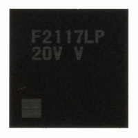
DF2117VLP20V Renesas Electronics America, DF2117VLP20V Datasheet - Page 659

DF2117VLP20V
Manufacturer Part Number
DF2117VLP20V
Description
IC H8S/2117 MCU FLASH 145TFLGA
Manufacturer
Renesas Electronics America
Series
H8® H8S/2100r
Datasheet
1.DF2117VBG20V.pdf
(960 pages)
Specifications of DF2117VLP20V
Core Processor
H8S/2600
Core Size
16-Bit
Speed
20MHz
Connectivity
FIFO, I²C, LPC, SCI, SmartCard
Peripherals
POR, PWM, WDT
Number Of I /o
112
Program Memory Size
160KB (160K x 8)
Program Memory Type
FLASH
Ram Size
8K x 8
Voltage - Supply (vcc/vdd)
3 V ~ 3.6 V
Data Converters
A/D 16x10b
Oscillator Type
External
Operating Temperature
-20°C ~ 75°C
Package / Case
145-TFLGA
For Use With
HS0005KCU11H - EMULATOR E10A-USB H8S(X),SH2(A)3DK2166 - DEV EVAL KIT H8S/2166
Lead Free Status / RoHS Status
Lead free / RoHS Compliant
Eeprom Size
-
Available stocks
Company
Part Number
Manufacturer
Quantity
Price
Company:
Part Number:
DF2117VLP20V
Manufacturer:
Renesas
Quantity:
100
Part Number:
DF2117VLP20V
Manufacturer:
RENESAS/瑞萨
Quantity:
20 000
- Current page: 659 of 960
- Download datasheet (6Mb)
19.3.11 Bidirectional Data Registers 0 to 15 (TWR0 to TWR15)
TWR0 to TWR15 are sixteen 8-bit readable/writable registers to both the slave (this LSI) and host.
In TWR0, however, two registers (TWR0MW and TWR0SW) are allocated to the same address
for both the host and the slave addresses. TWR0MW is a write-only register for the host, and a
read-only register for the slave, while TWR0SW is a write-only register for the slave and a read-
only register for the host. When the host and slave begin a write, after the respective registers of
TWR0 have been written to, arbitration for simultaneous access is performed by checking the
status flags whether or not those writes were valid.
When the host has access rights, TWR0MW is selected in TWR0 and the state of TWR0MW is
returned when the host reads TWR0SW. Attempts by the slave to write to TWR0SW are invalid.
When the slave has access rights, TWR0SW is selected in TWR0 and the state of TWR0SW is
returned when the slave reads TWR0MW. Attempts by the host to write to TWR0MW are invalid.
For the registers selected from the host according to the I/O address, see section 19.3.7, LPC
Channel 3 Address Registers H and L (LADR3H and LADR3L).
Data transferred in an LPC I/O write cycle is written to the selected register; in an LPC I/O read
cycle, the data in the selected register is transferred to the host. The initial values of TWR0 to
TWR15 are H'00.
19.3.12 Status Registers 1 to 4 (STR1 to STR4)
STR1 to STR4 are 8-bit registers that indicate status information during LPC interface processing.
The registers selected from the host according to the I/O address are shown in the following table.
In an LPC I/O read cycle, the data in the selected register is transferred to the host.
n = 1 to 4
Bits 15 to 4
Bits 15 to 4
Bit 3
Bit 3
I/O Address
Bit 2
1
Bit 1
Bit1
Bit 0
Bit 0
Transfer
Cycle
I/O read
Rev. 3.00 Sep. 28, 2009 Page 613 of 910
Section 19 LPC Interface (LPC)
STRn read
Host Register Selection
REJ09B0350-0300
Related parts for DF2117VLP20V
Image
Part Number
Description
Manufacturer
Datasheet
Request
R

Part Number:
Description:
KIT STARTER FOR M16C/29
Manufacturer:
Renesas Electronics America
Datasheet:

Part Number:
Description:
KIT STARTER FOR R8C/2D
Manufacturer:
Renesas Electronics America
Datasheet:

Part Number:
Description:
R0K33062P STARTER KIT
Manufacturer:
Renesas Electronics America
Datasheet:

Part Number:
Description:
KIT STARTER FOR R8C/23 E8A
Manufacturer:
Renesas Electronics America
Datasheet:

Part Number:
Description:
KIT STARTER FOR R8C/25
Manufacturer:
Renesas Electronics America
Datasheet:

Part Number:
Description:
KIT STARTER H8S2456 SHARPE DSPLY
Manufacturer:
Renesas Electronics America
Datasheet:

Part Number:
Description:
KIT STARTER FOR R8C38C
Manufacturer:
Renesas Electronics America
Datasheet:

Part Number:
Description:
KIT STARTER FOR R8C35C
Manufacturer:
Renesas Electronics America
Datasheet:

Part Number:
Description:
KIT STARTER FOR R8CL3AC+LCD APPS
Manufacturer:
Renesas Electronics America
Datasheet:

Part Number:
Description:
KIT STARTER FOR RX610
Manufacturer:
Renesas Electronics America
Datasheet:

Part Number:
Description:
KIT STARTER FOR R32C/118
Manufacturer:
Renesas Electronics America
Datasheet:

Part Number:
Description:
KIT DEV RSK-R8C/26-29
Manufacturer:
Renesas Electronics America
Datasheet:

Part Number:
Description:
KIT STARTER FOR SH7124
Manufacturer:
Renesas Electronics America
Datasheet:

Part Number:
Description:
KIT STARTER FOR H8SX/1622
Manufacturer:
Renesas Electronics America
Datasheet:

Part Number:
Description:
KIT DEV FOR SH7203
Manufacturer:
Renesas Electronics America
Datasheet:


