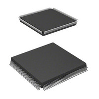
HD64F7051SFJ20V Renesas Electronics America, HD64F7051SFJ20V Datasheet - Page 191

HD64F7051SFJ20V
Manufacturer Part Number
HD64F7051SFJ20V
Description
MCU 5V 256K J-TEMP PB-FREE QFP-1
Manufacturer
Renesas Electronics America
Series
SuperH® SH7050r
Datasheet
1.HD64F7050SFJ20V.pdf
(843 pages)
Specifications of HD64F7051SFJ20V
Core Processor
SH-2
Core Size
32-Bit
Speed
20MHz
Connectivity
EBI/EMI, SCI
Peripherals
DMA, WDT
Number Of I /o
102
Program Memory Size
256KB (256K x 8)
Program Memory Type
FLASH
Ram Size
10K x 8
Voltage - Supply (vcc/vdd)
4.5 V ~ 5.5 V
Data Converters
A/D 16x10b
Oscillator Type
Internal
Operating Temperature
-40°C ~ 85°C
Package / Case
168-QFP
Lead Free Status / RoHS Status
Lead free / RoHS Compliant
Eeprom Size
-
Available stocks
Company
Part Number
Manufacturer
Quantity
Price
Company:
Part Number:
HD64F7051SFJ20V
Manufacturer:
RENESAS
Quantity:
101
Part Number:
HD64F7051SFJ20V
Manufacturer:
RENESAS/瑞萨
Quantity:
20 000
- Current page: 191 of 843
- Download datasheet (5Mb)
9.3.9
When a given channel is transferring in burst mode, and a transfer request is issued to channel 0,
which has a higher priority ranking, transfer on channel 0 begins immediately. If the priority level
setting is fixed mode (CH0
completely ended, whether the channel 0 setting is cycle steal mode or burst mode.
When the priority level setting is for round robin mode, transfer on channel 1 begins after transfer
of one transfer unit on channel 0, whether channel 0 is set to cycle steal mode or burst mode.
Thereafter, bus right alternates in the order: channel 1
Whether the priority level setting is for fixed mode or round robin mode, since channel 1 is set to
burst mode, the bus right is not given to the CPU. An example of round robin mode is shown in
figure 9.14.
9.3.10
Number of States in Bus Cycle: The number of states in the bus cycle when the DMAC is the
bus master is controlled by the bus state controller (BSC) just as it is when the CPU is the bus
master. The bus cycle in the dual address mode is controlled by wait state control register 1
(WCR1) while the single address mode bus cycle is controlled by wait state control register 2
(WCR2). For details, see section 8.3.2, Wait State Control.
DREQ
DREQ
DREQ
DREQ Pin Sampling Timing and DRAK Signal: In external request mode, the DREQ pin is
sampled by either falling edge or low-level detection. When a DREQ input is detected, a DMAC
bus cycle is issued and DMA transfer effected, at the earliest, after three states. However, in burst
mode when single address operation is specified, a dummy cycle is inserted for the first bus cycle.
In this case, the actual data transfer starts from the second bus cycle. Data is transferred
Priority: Round-robin mode
ch0: Cycle-steal mode
ch1: Burst mode
CPU
CPU
Bus Mode and Channel Priority Order
Number of Bus Cycle States and DREQ
Figure 9.14 Bus Handling when Multiple Channels Are Operating
DMAC
ch1
burst mode
DMAC ch1
DMAC
ch1
CH1), channel 1 transfer is continued after transfer on channel 0 are
DMAC
ch0
ch0
DMAC ch0 and ch1
round-robin mode
DREQ
DREQ
DREQ Pin Sample Timing
Section 9 Direct Memory Access Controller (DMAC)
DMAC
ch1
ch1
DMAC
channel 0
ch0
Rev. 5.00 Jan 06, 2006 page 169 of 818
ch0
DMAC
ch1
burst mode
DMAC ch1
channel 1
DMAC
ch1
REJ09B0273-0500
channel 0.
CPU
CPU
Related parts for HD64F7051SFJ20V
Image
Part Number
Description
Manufacturer
Datasheet
Request
R

Part Number:
Description:
KIT STARTER FOR M16C/29
Manufacturer:
Renesas Electronics America
Datasheet:

Part Number:
Description:
KIT STARTER FOR R8C/2D
Manufacturer:
Renesas Electronics America
Datasheet:

Part Number:
Description:
R0K33062P STARTER KIT
Manufacturer:
Renesas Electronics America
Datasheet:

Part Number:
Description:
KIT STARTER FOR R8C/23 E8A
Manufacturer:
Renesas Electronics America
Datasheet:

Part Number:
Description:
KIT STARTER FOR R8C/25
Manufacturer:
Renesas Electronics America
Datasheet:

Part Number:
Description:
KIT STARTER H8S2456 SHARPE DSPLY
Manufacturer:
Renesas Electronics America
Datasheet:

Part Number:
Description:
KIT STARTER FOR R8C38C
Manufacturer:
Renesas Electronics America
Datasheet:

Part Number:
Description:
KIT STARTER FOR R8C35C
Manufacturer:
Renesas Electronics America
Datasheet:

Part Number:
Description:
KIT STARTER FOR R8CL3AC+LCD APPS
Manufacturer:
Renesas Electronics America
Datasheet:

Part Number:
Description:
KIT STARTER FOR RX610
Manufacturer:
Renesas Electronics America
Datasheet:

Part Number:
Description:
KIT STARTER FOR R32C/118
Manufacturer:
Renesas Electronics America
Datasheet:

Part Number:
Description:
KIT DEV RSK-R8C/26-29
Manufacturer:
Renesas Electronics America
Datasheet:

Part Number:
Description:
KIT STARTER FOR SH7124
Manufacturer:
Renesas Electronics America
Datasheet:

Part Number:
Description:
KIT STARTER FOR H8SX/1622
Manufacturer:
Renesas Electronics America
Datasheet:

Part Number:
Description:
KIT DEV FOR SH7203
Manufacturer:
Renesas Electronics America
Datasheet:


