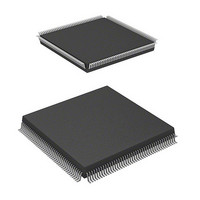
HD64F7051SFJ20V Renesas Electronics America, HD64F7051SFJ20V Datasheet - Page 651

HD64F7051SFJ20V
Manufacturer Part Number
HD64F7051SFJ20V
Description
MCU 5V 256K J-TEMP PB-FREE QFP-1
Manufacturer
Renesas Electronics America
Series
SuperH® SH7050r
Datasheet
1.HD64F7050SFJ20V.pdf
(843 pages)
Specifications of HD64F7051SFJ20V
Core Processor
SH-2
Core Size
32-Bit
Speed
20MHz
Connectivity
EBI/EMI, SCI
Peripherals
DMA, WDT
Number Of I /o
102
Program Memory Size
256KB (256K x 8)
Program Memory Type
FLASH
Ram Size
10K x 8
Voltage - Supply (vcc/vdd)
4.5 V ~ 5.5 V
Data Converters
A/D 16x10b
Oscillator Type
Internal
Operating Temperature
-40°C ~ 85°C
Package / Case
168-QFP
Lead Free Status / RoHS Status
Lead free / RoHS Compliant
Eeprom Size
-
Available stocks
Company
Part Number
Manufacturer
Quantity
Price
Company:
Part Number:
HD64F7051SFJ20V
Manufacturer:
RENESAS
Quantity:
101
Part Number:
HD64F7051SFJ20V
Manufacturer:
RENESAS/瑞萨
Quantity:
20 000
- Current page: 651 of 843
- Download datasheet (5Mb)
19.11.4 Auto-Program Mode
1. In auto-program mode, 128 bytes are programmed simultaneously. This should be carried out
2. A 128-byte data transfer is necessary even when programming fewer than 128 bytes. In this
3. The lower 7 bits of the transfer address must be low. If a value other than an effective address
4. Memory address transfer is performed in the third cycle (figure 18.13). Do not perform transfer
5. Do not perform a command write during a programming operation.
6. Perform one auto-program operation for a 128-byte block for each address. Two or more
7. Confirm normal end of auto-programming by checking D6. Alternatively, status read mode
8. Status polling D6 and D7 pin information is retained until the next command write. As long as
I/O7–I/O0
by executing 128 consecutive byte transfers.
case, H'FF data must be written to the extra addresses.
is input, processing will switch to a memory write operation but a write error will be flagged.
after the second cycle.
additional programming operations cannot be performed on a previously programmed address
block.
can also be used for this purpose (D7 status polling uses the auto-program operation end
identification pin).
the next command write has not been performed, reading is possible by enabling CE and OE.
A16–A0
WE
OE
CE
Figure 19.17 CE
V
IH
Address stable
t
acc
CE
CE and OE
CE
t
ce
t
oe
OE
OE Clock System Read Timing Waveforms
OE
t
oh
t
df
Rev. 5.00 Jan 06, 2006 page 629 of 818
Address stable
t
acc
Section 19 ROM (256 kB Version)
t
ce
t
oe
REJ09B0273-0500
t
oh
t
df
Related parts for HD64F7051SFJ20V
Image
Part Number
Description
Manufacturer
Datasheet
Request
R

Part Number:
Description:
KIT STARTER FOR M16C/29
Manufacturer:
Renesas Electronics America
Datasheet:

Part Number:
Description:
KIT STARTER FOR R8C/2D
Manufacturer:
Renesas Electronics America
Datasheet:

Part Number:
Description:
R0K33062P STARTER KIT
Manufacturer:
Renesas Electronics America
Datasheet:

Part Number:
Description:
KIT STARTER FOR R8C/23 E8A
Manufacturer:
Renesas Electronics America
Datasheet:

Part Number:
Description:
KIT STARTER FOR R8C/25
Manufacturer:
Renesas Electronics America
Datasheet:

Part Number:
Description:
KIT STARTER H8S2456 SHARPE DSPLY
Manufacturer:
Renesas Electronics America
Datasheet:

Part Number:
Description:
KIT STARTER FOR R8C38C
Manufacturer:
Renesas Electronics America
Datasheet:

Part Number:
Description:
KIT STARTER FOR R8C35C
Manufacturer:
Renesas Electronics America
Datasheet:

Part Number:
Description:
KIT STARTER FOR R8CL3AC+LCD APPS
Manufacturer:
Renesas Electronics America
Datasheet:

Part Number:
Description:
KIT STARTER FOR RX610
Manufacturer:
Renesas Electronics America
Datasheet:

Part Number:
Description:
KIT STARTER FOR R32C/118
Manufacturer:
Renesas Electronics America
Datasheet:

Part Number:
Description:
KIT DEV RSK-R8C/26-29
Manufacturer:
Renesas Electronics America
Datasheet:

Part Number:
Description:
KIT STARTER FOR SH7124
Manufacturer:
Renesas Electronics America
Datasheet:

Part Number:
Description:
KIT STARTER FOR H8SX/1622
Manufacturer:
Renesas Electronics America
Datasheet:

Part Number:
Description:
KIT DEV FOR SH7203
Manufacturer:
Renesas Electronics America
Datasheet:


