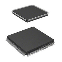
HD64F7051SFJ20V Renesas Electronics America, HD64F7051SFJ20V Datasheet - Page 314

HD64F7051SFJ20V
Manufacturer Part Number
HD64F7051SFJ20V
Description
MCU 5V 256K J-TEMP PB-FREE QFP-1
Manufacturer
Renesas Electronics America
Series
SuperH® SH7050r
Datasheet
1.HD64F7050SFJ20V.pdf
(843 pages)
Specifications of HD64F7051SFJ20V
Core Processor
SH-2
Core Size
32-Bit
Speed
20MHz
Connectivity
EBI/EMI, SCI
Peripherals
DMA, WDT
Number Of I /o
102
Program Memory Size
256KB (256K x 8)
Program Memory Type
FLASH
Ram Size
10K x 8
Voltage - Supply (vcc/vdd)
4.5 V ~ 5.5 V
Data Converters
A/D 16x10b
Oscillator Type
Internal
Operating Temperature
-40°C ~ 85°C
Package / Case
168-QFP
Lead Free Status / RoHS Status
Lead free / RoHS Compliant
Eeprom Size
-
Available stocks
Company
Part Number
Manufacturer
Quantity
Price
Company:
Part Number:
HD64F7051SFJ20V
Manufacturer:
RENESAS
Quantity:
101
Part Number:
HD64F7051SFJ20V
Manufacturer:
RENESAS/瑞萨
Quantity:
20 000
- Current page: 314 of 843
- Download datasheet (5Mb)
Section 10 Advanced Timer Unit (ATU)
10.3.7
Interval Timer Operation
The 8 bits of the interval interrupt request register (ITVRR) are connected to bits 10 to 13 of
TCNT0L in the channel 0 32-bit free-running counter (TCNT0H, TCNT0L). The upper 4 bits
(ITVAD3 to ITVAD0) are used to start A/D converter sampling, and the lower 4 bits (ITVE3 to
ITVE0) generate signals to the interrupt controller (INTC).
For A/D converter activation, an edge sensor is provided for bits 10 to 13 of TCNT0L, and A/D
channel 0 sampling is started when the corresponding bit in TCNT0L changes to 1 as a result of
setting 1 in one of the upper 4 bits (ITVAD3 to ITVAD0) of ITVRR.
For generation of interrupt signals to the INTC, after detection of bits 10 to 13 of TCNT0L by the
edge sensor, when the corresponding bit in TCNT0L changes to 1 as a result of setting 1 in one of
the lower 4 bits (ITVE3 to ITVE0) of ITVRR after detection of bits 10 to 13 of TCNT0L by the
edge sensor, the corresponding flag (IIF0 to IIF3) in timer status register TSRAH is set to 1 and an
interrupt request is sent to INTC. The above four interrupt sources have only one interrupt vector
address, and therefore when more than one of bits ITVE3 to ITVE0 in ITVRR is specified, control
branches to the same vector when any TCNT0 bit corresponding to one of the specified bits
changes to 1.
To suppress interrupts to INTC, or to prevent A/D sampling from being started, all ITVRR bits
should be cleared to 0.
A schematic diagram of the interval timer is shown in figure 10.17.
Rev. 5.00 Jan 06, 2006 page 292 of 818
REJ09B0273-0500
Related parts for HD64F7051SFJ20V
Image
Part Number
Description
Manufacturer
Datasheet
Request
R

Part Number:
Description:
KIT STARTER FOR M16C/29
Manufacturer:
Renesas Electronics America
Datasheet:

Part Number:
Description:
KIT STARTER FOR R8C/2D
Manufacturer:
Renesas Electronics America
Datasheet:

Part Number:
Description:
R0K33062P STARTER KIT
Manufacturer:
Renesas Electronics America
Datasheet:

Part Number:
Description:
KIT STARTER FOR R8C/23 E8A
Manufacturer:
Renesas Electronics America
Datasheet:

Part Number:
Description:
KIT STARTER FOR R8C/25
Manufacturer:
Renesas Electronics America
Datasheet:

Part Number:
Description:
KIT STARTER H8S2456 SHARPE DSPLY
Manufacturer:
Renesas Electronics America
Datasheet:

Part Number:
Description:
KIT STARTER FOR R8C38C
Manufacturer:
Renesas Electronics America
Datasheet:

Part Number:
Description:
KIT STARTER FOR R8C35C
Manufacturer:
Renesas Electronics America
Datasheet:

Part Number:
Description:
KIT STARTER FOR R8CL3AC+LCD APPS
Manufacturer:
Renesas Electronics America
Datasheet:

Part Number:
Description:
KIT STARTER FOR RX610
Manufacturer:
Renesas Electronics America
Datasheet:

Part Number:
Description:
KIT STARTER FOR R32C/118
Manufacturer:
Renesas Electronics America
Datasheet:

Part Number:
Description:
KIT DEV RSK-R8C/26-29
Manufacturer:
Renesas Electronics America
Datasheet:

Part Number:
Description:
KIT STARTER FOR SH7124
Manufacturer:
Renesas Electronics America
Datasheet:

Part Number:
Description:
KIT STARTER FOR H8SX/1622
Manufacturer:
Renesas Electronics America
Datasheet:

Part Number:
Description:
KIT DEV FOR SH7203
Manufacturer:
Renesas Electronics America
Datasheet:


