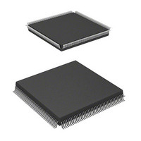
HD64F7051SFJ20V Renesas Electronics America, HD64F7051SFJ20V Datasheet - Page 449

HD64F7051SFJ20V
Manufacturer Part Number
HD64F7051SFJ20V
Description
MCU 5V 256K J-TEMP PB-FREE QFP-1
Manufacturer
Renesas Electronics America
Series
SuperH® SH7050r
Datasheet
1.HD64F7050SFJ20V.pdf
(843 pages)
Specifications of HD64F7051SFJ20V
Core Processor
SH-2
Core Size
32-Bit
Speed
20MHz
Connectivity
EBI/EMI, SCI
Peripherals
DMA, WDT
Number Of I /o
102
Program Memory Size
256KB (256K x 8)
Program Memory Type
FLASH
Ram Size
10K x 8
Voltage - Supply (vcc/vdd)
4.5 V ~ 5.5 V
Data Converters
A/D 16x10b
Oscillator Type
Internal
Operating Temperature
-40°C ~ 85°C
Package / Case
168-QFP
Lead Free Status / RoHS Status
Lead free / RoHS Compliant
Eeprom Size
-
Available stocks
Company
Part Number
Manufacturer
Quantity
Price
Company:
Part Number:
HD64F7051SFJ20V
Manufacturer:
RENESAS
Quantity:
101
Part Number:
HD64F7051SFJ20V
Manufacturer:
RENESAS/瑞萨
Quantity:
20 000
- Current page: 449 of 843
- Download datasheet (5Mb)
13.5.3
Break signals can be detected by reading the RxD pin directly when a framing error (FER) is
detected. In the break state, the input from the RxD pin consists of all 0s, so FER is set and the
parity error flag (PER) may also be set. In the break state, the SCI receiver continues to operate, so
if the FER bit is cleared to 0, it will be set to 1 again.
13.5.4
The TxD pin becomes a general I/O pin with the I/O direction and level determined by the I/O port
data register (DR) and pin function controller (PFC) control register (CR). These conditions allow
break signals to be sent. The DR value is substituted for the marking status until the PFC is set.
Consequently, the output port is set to initially output a 1. To send a break in serial transmission,
first clear the DR to 0, then establish the TxD pin as an output port using the PFC. When TE is
cleared to 0, the transmission section is initialized regardless of the present transmission status.
13.5.5
When a receive error flag (ORER, PER, or FER) is set to 1, the SCI will not start transmitting
even if TDRE is set to 1. Be sure to clear the receive error flags to 0 before starting to transmit.
Note that clearing RE to 0 does not clear the receive error flags.
13.5.6
In the asynchronous mode, the SCI operates on a base clock of 16 times the bit rate frequency. In
receiving, the SCI synchronizes internally with the falling edge of the start bit, which it samples
on the base clock. Receive data is latched on the rising edge of the eighth base clock pulse (figure
13.23).
Break Detection and Processing
Sending a Break Signal
Receive Error Flags and Transmitter Operation (Clock Synchronous Mode Only)
Receive Data Sampling Timing and Receive Margin in the Asynchronous Mode
Section 13 Serial Communication Interface (SCI)
Rev. 5.00 Jan 06, 2006 page 427 of 818
REJ09B0273-0500
Related parts for HD64F7051SFJ20V
Image
Part Number
Description
Manufacturer
Datasheet
Request
R

Part Number:
Description:
KIT STARTER FOR M16C/29
Manufacturer:
Renesas Electronics America
Datasheet:

Part Number:
Description:
KIT STARTER FOR R8C/2D
Manufacturer:
Renesas Electronics America
Datasheet:

Part Number:
Description:
R0K33062P STARTER KIT
Manufacturer:
Renesas Electronics America
Datasheet:

Part Number:
Description:
KIT STARTER FOR R8C/23 E8A
Manufacturer:
Renesas Electronics America
Datasheet:

Part Number:
Description:
KIT STARTER FOR R8C/25
Manufacturer:
Renesas Electronics America
Datasheet:

Part Number:
Description:
KIT STARTER H8S2456 SHARPE DSPLY
Manufacturer:
Renesas Electronics America
Datasheet:

Part Number:
Description:
KIT STARTER FOR R8C38C
Manufacturer:
Renesas Electronics America
Datasheet:

Part Number:
Description:
KIT STARTER FOR R8C35C
Manufacturer:
Renesas Electronics America
Datasheet:

Part Number:
Description:
KIT STARTER FOR R8CL3AC+LCD APPS
Manufacturer:
Renesas Electronics America
Datasheet:

Part Number:
Description:
KIT STARTER FOR RX610
Manufacturer:
Renesas Electronics America
Datasheet:

Part Number:
Description:
KIT STARTER FOR R32C/118
Manufacturer:
Renesas Electronics America
Datasheet:

Part Number:
Description:
KIT DEV RSK-R8C/26-29
Manufacturer:
Renesas Electronics America
Datasheet:

Part Number:
Description:
KIT STARTER FOR SH7124
Manufacturer:
Renesas Electronics America
Datasheet:

Part Number:
Description:
KIT STARTER FOR H8SX/1622
Manufacturer:
Renesas Electronics America
Datasheet:

Part Number:
Description:
KIT DEV FOR SH7203
Manufacturer:
Renesas Electronics America
Datasheet:


