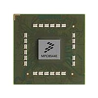
MPC8544DS Freescale Semiconductor, MPC8544DS Datasheet - Page 280

MPC8544DS
Manufacturer Part Number
MPC8544DS
Description
BOARD DEVELOPMENT SYSTEM 8544
Manufacturer
Freescale Semiconductor
Series
PowerQUICC III™r
Type
MPUr
Datasheets
1.MPC8544VTALF.pdf
(117 pages)
2.MPC8544VTALF.pdf
(2 pages)
3.MPC8544VTALF.pdf
(1340 pages)
4.MPC8544DS.pdf
(2 pages)
Specifications of MPC8544DS
Contents
Board
Processor To Be Evaluated
MPC8544E
Data Bus Width
32 bit
Interface Type
Ethernet, I2C
Operating Supply Voltage
- 0.3 V to + 1.1 V
Leaded Process Compatible
Yes
Peak Reflow Compatible (260 C)
Yes
Rohs Compliant
Yes
For Use With/related Products
MPC8544
For Use With
PPC8544EVTANG - EVAL MPC8544 783FCPBGA
Lead Free Status / RoHS Status
Lead free / RoHS Compliant
- MPC8544VTALF PDF datasheet
- MPC8544VTALF PDF datasheet #2
- MPC8544VTALF PDF datasheet #3
- MPC8544DS PDF datasheet #4
- Current page: 280 of 1340
- Download datasheet (12Mb)
L2 Look-Aside Cache/SRAM
7.3.1
The following sections describe registers that control and configure the L2/SRAM array.
7.3.1.1
The L2 control register (L2CTL), shown in
L2/SRAM array. The sequence for modifying L2CTL is as follows:
Table 7-4
7-10
Offset 0x2_0000
Reset
Reset
Bits
2–3
0
1
1. mbar
2. isync
3. stw (WIMG = 01xx) CCSRBAR+0x2_0000
4. lwz (WIMG = 01xx) CCSRBAR+0x2_0000
5. mbar
W
W
R
R
L2E
16
0
0
describes L2CTL fields.
Name
L2SIZ
—
L2E
L2I
L2/SRAM Register Descriptions
L2I
MPC8544E PowerQUICC III Integrated Host Processor Family Reference Manual, Rev. 1
17
0
1
L2 Control Register (L2CTL)
L2LO L2SLC
18
2
1
L2 enable. Used to enable the L2 array (cache or memory-mapped SRAM).
0 The L2 SRAM (cache and memory-mapped SRAM) is disabled and is not accessed for reads,
1 The L2 SRAM (cache or memory-mapped SRAM) is enabled.
Note that L2I can be set regardless of the value of L2E.
L2 flash invalidate.
0 The L2 status and LRU bits are not being cleared.
1 Setting L2I invalidates the L2 cache globally by clearing the all the L2 status bits, as well as the LRU
Data to memory-mapped SRAM are unaffected by the flash invalidate. The hardware automatically
clears L2I when the invalidate is complete.
L2 SRAM size (read only). Indicates the total available size of on-chip memory array (to be configured
as cache or memory-mapped SRAM).
00 Reserved
01 256 Kbyte
10 Reserved
11 Reserved
L2SIZ
snoops, or writes. Setting the L2 flash invalidate bit (L2I) is allowed.
algorithm. Memory-mapped SRAM is unaffected.
19
0
3
—
20
4
0
Figure 7-7. L2 Control Register (L2CTL)
Table 7-4. L2CTL Field Descriptions
L2LFR L2LFRID
21
0
—
22
Figure
0
23
0
7-7, controls configuration and operation of the
All zeros
24
8
0
L2DO L2IO
Description
0
9
—
10
0
—
11
27
0
L2STASHDIS
L2INTDIS
12
28
0
Freescale Semiconductor
Access: Read/Write
—
13
29
0
L2SRAM
L2STASHCTL
30
0
15
31
0
Related parts for MPC8544DS
Image
Part Number
Description
Manufacturer
Datasheet
Request
R
Part Number:
Description:
Manufacturer:
Freescale Semiconductor, Inc
Datasheet:
Part Number:
Description:
Manufacturer:
Freescale Semiconductor, Inc
Datasheet:
Part Number:
Description:
Manufacturer:
Freescale Semiconductor, Inc
Datasheet:
Part Number:
Description:
Manufacturer:
Freescale Semiconductor, Inc
Datasheet:
Part Number:
Description:
Manufacturer:
Freescale Semiconductor, Inc
Datasheet:
Part Number:
Description:
Manufacturer:
Freescale Semiconductor, Inc
Datasheet:
Part Number:
Description:
Manufacturer:
Freescale Semiconductor, Inc
Datasheet:
Part Number:
Description:
Manufacturer:
Freescale Semiconductor, Inc
Datasheet:
Part Number:
Description:
Manufacturer:
Freescale Semiconductor, Inc
Datasheet:
Part Number:
Description:
Manufacturer:
Freescale Semiconductor, Inc
Datasheet:
Part Number:
Description:
Manufacturer:
Freescale Semiconductor, Inc
Datasheet:
Part Number:
Description:
Manufacturer:
Freescale Semiconductor, Inc
Datasheet:
Part Number:
Description:
Manufacturer:
Freescale Semiconductor, Inc
Datasheet:
Part Number:
Description:
Manufacturer:
Freescale Semiconductor, Inc
Datasheet:
Part Number:
Description:
Manufacturer:
Freescale Semiconductor, Inc
Datasheet:


