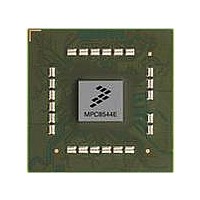
MPC8544DS Freescale Semiconductor, MPC8544DS Datasheet - Page 338

MPC8544DS
Manufacturer Part Number
MPC8544DS
Description
BOARD DEVELOPMENT SYSTEM 8544
Manufacturer
Freescale Semiconductor
Series
PowerQUICC III™r
Type
MPUr
Datasheets
1.MPC8544VTALF.pdf
(117 pages)
2.MPC8544VTALF.pdf
(2 pages)
3.MPC8544VTALF.pdf
(1340 pages)
4.MPC8544DS.pdf
(2 pages)
Specifications of MPC8544DS
Contents
Board
Processor To Be Evaluated
MPC8544E
Data Bus Width
32 bit
Interface Type
Ethernet, I2C
Operating Supply Voltage
- 0.3 V to + 1.1 V
Leaded Process Compatible
Yes
Peak Reflow Compatible (260 C)
Yes
Rohs Compliant
Yes
For Use With/related Products
MPC8544
For Use With
PPC8544EVTANG - EVAL MPC8544 783FCPBGA
Lead Free Status / RoHS Status
Lead free / RoHS Compliant
- MPC8544VTALF PDF datasheet
- MPC8544VTALF PDF datasheet #2
- MPC8544VTALF PDF datasheet #3
- MPC8544DS PDF datasheet #4
- Current page: 338 of 1340
- Download datasheet (12Mb)
DDR Memory Controller
Table 9-8
9.4.1.4
DDR SDRAM timing configuration register 0, shown in
between various SDRAM control commands.
Table 9-9
9-14
13–15
16–31
Offset 0x104
Reset 0 0
0–12
Bits
Bits
0–1
W
R
RWT WRT RRT
0
EXT_REFREC
1
describes TIMING_CFG_3 fields.
describes TIMING_CFG_0 fields.
Name
Name
0 0 0
2
RWT
DDR SDRAM Timing Configuration 0 (TIMING_CFG_0)
—
—
MPC8544E PowerQUICC III Integrated Host Processor Family Reference Manual, Rev. 1
3 4
Figure 9-5. DDR SDRAM Timing Configuration 0 (TIMING_CFG_0)
0
5
Read-to-write turnaround (t
write turnaround. If 0 clocks is chosen, then the DDR controller will use a fixed number based on the
CAS latency and write latency. Choosing a value other than 0 adds extra cycles past this default
calculation. As a default the DDR controller will determine the read-to-write turnaround as CL – WL
+ BL/2 + 2. In this equation, CL is the CAS latency rounded up to the next integer, WL is the
programmed write latency, and BL is the burst length.
00 0 clocks
01 1 clock
Reserved, should be cleared.
Extended refresh recovery time (t
until an activate command is allowed. This field is concatenated with TIMING_CFG_1[REFREC] to
obtain a 7bit value for the total refresh recovery. Note that hardware adds an additional 8 clock cycles
to the final, 7bit value of the refresh recovery. t
is calculated as follows:
000 0 clocks
001 16 clocks
010 32 clocks
011 48 clocks
100 64 clocks
101 80 clocks
110 96 clocks
111 112 clocks
Reserved, should be cleared.
WWT — ACT_PD_EXIT — PRE_PD_EXIT
0
6
0
7
Table 9-8. TIMING_CFG_3 Field Descriptions
8
0
Table 9-9. TIMING_CFG_0 Field Descriptions
0
9
0
11
1
RTW
12
0
). Specifies how many extra cycles will be added between a read to
RFC
13
0
). Controls the number of clock cycles from a refresh command
0
Figure
Description
Description
15
1
RFC
16
0 0 0 0
9-5, sets the number of clock cycles
10 2 clocks
11 3 clocks
= {EXT_REFREC || REFREC} + 8, such that t
—
19 20
ODT_PD_EXIT
0
0
0
23 24
1
Freescale Semiconductor
0 0 0 0 0 1 0 1
Access: Read/Write
—
27 28
MRS_CYC
RFC
31
Related parts for MPC8544DS
Image
Part Number
Description
Manufacturer
Datasheet
Request
R
Part Number:
Description:
Manufacturer:
Freescale Semiconductor, Inc
Datasheet:
Part Number:
Description:
Manufacturer:
Freescale Semiconductor, Inc
Datasheet:
Part Number:
Description:
Manufacturer:
Freescale Semiconductor, Inc
Datasheet:
Part Number:
Description:
Manufacturer:
Freescale Semiconductor, Inc
Datasheet:
Part Number:
Description:
Manufacturer:
Freescale Semiconductor, Inc
Datasheet:
Part Number:
Description:
Manufacturer:
Freescale Semiconductor, Inc
Datasheet:
Part Number:
Description:
Manufacturer:
Freescale Semiconductor, Inc
Datasheet:
Part Number:
Description:
Manufacturer:
Freescale Semiconductor, Inc
Datasheet:
Part Number:
Description:
Manufacturer:
Freescale Semiconductor, Inc
Datasheet:
Part Number:
Description:
Manufacturer:
Freescale Semiconductor, Inc
Datasheet:
Part Number:
Description:
Manufacturer:
Freescale Semiconductor, Inc
Datasheet:
Part Number:
Description:
Manufacturer:
Freescale Semiconductor, Inc
Datasheet:
Part Number:
Description:
Manufacturer:
Freescale Semiconductor, Inc
Datasheet:
Part Number:
Description:
Manufacturer:
Freescale Semiconductor, Inc
Datasheet:
Part Number:
Description:
Manufacturer:
Freescale Semiconductor, Inc
Datasheet:


