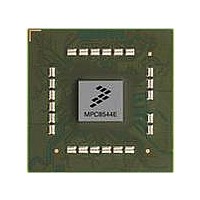
MPC8544DS Freescale Semiconductor, MPC8544DS Datasheet - Page 344

MPC8544DS
Manufacturer Part Number
MPC8544DS
Description
BOARD DEVELOPMENT SYSTEM 8544
Manufacturer
Freescale Semiconductor
Series
PowerQUICC III™r
Type
MPUr
Datasheets
1.MPC8544VTALF.pdf
(117 pages)
2.MPC8544VTALF.pdf
(2 pages)
3.MPC8544VTALF.pdf
(1340 pages)
4.MPC8544DS.pdf
(2 pages)
Specifications of MPC8544DS
Contents
Board
Processor To Be Evaluated
MPC8544E
Data Bus Width
32 bit
Interface Type
Ethernet, I2C
Operating Supply Voltage
- 0.3 V to + 1.1 V
Leaded Process Compatible
Yes
Peak Reflow Compatible (260 C)
Yes
Rohs Compliant
Yes
For Use With/related Products
MPC8544
For Use With
PPC8544EVTANG - EVAL MPC8544 783FCPBGA
Lead Free Status / RoHS Status
Lead free / RoHS Compliant
- MPC8544VTALF PDF datasheet
- MPC8544VTALF PDF datasheet #2
- MPC8544VTALF PDF datasheet #3
- MPC8544DS PDF datasheet #4
- Current page: 344 of 1340
- Download datasheet (12Mb)
1
19–21 WR_DATA_DELAY Write command to write data strobe timing adjustment. Controls the amount of delay applied to the
23–25
26–31
DDR Memory Controller
9.4.1.7
The DDR SDRAM control configuration register, shown in
specifies certain operating features such as self refreshing, error checking and correcting, registered
DIMMs, and dynamic power management.
9-20
Offset 0x110
Reset
Reset
Bits
22
For CPO decodings other than 00000 and 11111, ‘READ_LAT’ is rounded up to the next integer value.
W
W
R
R
MEM_EN SREN ECC_EN RD_EN — SDRAM_TYPE
2T_EN
FOUR_ACT
16
0
0
CKE_PLS
Name
DDR SDRAM Control Configuration (DDR_SDRAM_CFG)
—
MPC8544E PowerQUICC III Integrated Host Processor Family Reference Manual, Rev. 1
Figure 9-8. DDR SDRAM Control Configuration Register (DDR_SDRAM_CFG)
17
0
1
Table 9-11. TIMING_CFG_2 Field Descriptions (continued)
data and data strobes for writes. See
details.
000 0 clock delay
001 1/4 clock delay
010 1/2 clock delay
011 3/4 clock delay
Reserved
Minimum CKE pulse width (t
000 Reserved
001 1 cycle
010 2 cycles
Window for four activates (t
to 000001 for DDR1.
000000 Reserved
000001 1 cycle
000010 2 cycles
000011 3 cycles
000100 4 cycles
0
2
BA_INTLV_CTL
0
3
0
4
0
5
1
FAW
CKE
). This is applied to DDR2 with eight logical banks only. Must be set
). Can be set to 001 for DDR1.
23
0
7
All zeros
24 25
0 0
8
Section 9.5.7, “DDR SDRAM Write Timing Adjustments,”
—
—
9
100 1 clock delay
101 5/4 clock delay
110 3/2 clock delay
111 Reserved
011 3 cycles
100 4 cycles
101–111 Reserved
...
010011 19 cycles
010100 20 cycles
010101–111111 Reserved
Description
DYN_PWR
Figure
x32_EN
10
26
0
9-8, enables the interface logic and
PCHB8 HSE
11
—
27
0
32_BE 8_BE
12
28
0
Freescale Semiconductor
—
13
29
0
Access: Read/Write
MEM_HALT
NCAP
14
30
0
—
BI
15
31
0
for
Related parts for MPC8544DS
Image
Part Number
Description
Manufacturer
Datasheet
Request
R
Part Number:
Description:
Manufacturer:
Freescale Semiconductor, Inc
Datasheet:
Part Number:
Description:
Manufacturer:
Freescale Semiconductor, Inc
Datasheet:
Part Number:
Description:
Manufacturer:
Freescale Semiconductor, Inc
Datasheet:
Part Number:
Description:
Manufacturer:
Freescale Semiconductor, Inc
Datasheet:
Part Number:
Description:
Manufacturer:
Freescale Semiconductor, Inc
Datasheet:
Part Number:
Description:
Manufacturer:
Freescale Semiconductor, Inc
Datasheet:
Part Number:
Description:
Manufacturer:
Freescale Semiconductor, Inc
Datasheet:
Part Number:
Description:
Manufacturer:
Freescale Semiconductor, Inc
Datasheet:
Part Number:
Description:
Manufacturer:
Freescale Semiconductor, Inc
Datasheet:
Part Number:
Description:
Manufacturer:
Freescale Semiconductor, Inc
Datasheet:
Part Number:
Description:
Manufacturer:
Freescale Semiconductor, Inc
Datasheet:
Part Number:
Description:
Manufacturer:
Freescale Semiconductor, Inc
Datasheet:
Part Number:
Description:
Manufacturer:
Freescale Semiconductor, Inc
Datasheet:
Part Number:
Description:
Manufacturer:
Freescale Semiconductor, Inc
Datasheet:
Part Number:
Description:
Manufacturer:
Freescale Semiconductor, Inc
Datasheet:


