MPC8544DS Freescale Semiconductor, MPC8544DS Datasheet - Page 395
MPC8544DS
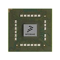
Manufacturer Part Number
MPC8544DS
Description
BOARD DEVELOPMENT SYSTEM 8544
Manufacturer
Freescale Semiconductor
Series
PowerQUICC III™r
Type
MPUr
Datasheets
1.MPC8544VTALF.pdf
(117 pages)
2.MPC8544VTALF.pdf
(2 pages)
3.MPC8544VTALF.pdf
(1340 pages)
4.MPC8544DS.pdf
(2 pages)
Specifications of MPC8544DS
Contents
Board
Processor To Be Evaluated
MPC8544E
Data Bus Width
32 bit
Interface Type
Ethernet, I2C
Operating Supply Voltage
- 0.3 V to + 1.1 V
Leaded Process Compatible
Yes
Peak Reflow Compatible (260 C)
Yes
Rohs Compliant
Yes
For Use With/related Products
MPC8544
For Use With
PPC8544EVTANG - EVAL MPC8544 783FCPBGA
Lead Free Status / RoHS Status
Lead free / RoHS Compliant


Freescale Semiconductor
RD_TO_PRE
FOUR_ACT
Parameter
WRTORD
CKE_PLS
ADD_LAT
WR_LAT
RD_EN
2T_EN
8_BE
MPC8544E PowerQUICC III Integrated Host Processor Family Reference Manual, Rev. 1
Table 9-54. Programming Differences Between Memory Types (continued)
Write to Read Timing
Additive Latency
Write Latency
Read to Precharge Timing
Minimum CKE Pulse Width DDR1
Four Activate Window
Registered DIMM Enable
8-beat burst enable
2T Timing Enable
Description
DDR2
DDR1
DDR2
DDR1
DDR2
DDR2
DDR2
DDR2
DDR2
DDR1
DDR2
DDR2
DDR1
DDR1
DDR1
DDR1
DDR1
the memory used (t
the memory used (t
Should be set to 000
must be set to a value less than
TIMING_CFG_1[ACTTORW]
Should be set to 001
Should be set to CAS latency – 1 cycle. For
example, if the CAS latency if 5 cycles, then this
field should be set to 100 (4 cycles).
burst length is 8
the memory used (t
precharge for non-zero value of additive latency
(AL) is a minimum of AL + t
the memory used (t
the memory used (t
logical banks.
should be set to 1
If registered DIMMs are used, then this field
should be set to 1
desired, then this field should be set to 1
Should be set to 0
gain extra timing margin on the interface at the
cost of address/command bandwidth.
gain extra timing margin on the interface at the
cost of address/command bandwidth.
Should be set according to the specifications for
Should be set according to the specifications for
Should be set to the desired additive latency. This
Should be set to 010 if burst length is 4 and 100 if
Should be set according to the specifications for
Can be set to 001
Should be set according to the specifications for
Should be set to 0001
Should be set according to the specifications for
If registered DIMMs are used, then this field
If a 32-bit bus is used, and 8-beat bursts are
In heavily loaded systems, this can be set to 1 to
In heavily loaded systems, this can be set to 1 to
Differences
RTP
WRD
WRD
CKE
FAW
). Time between read and
)
). Only applies to eight
)
)
RTP
cycles.
DDR Memory Controller
Section/page
9.4.1.5/9-16
9.4.1.6/9-18
9.4.1.6/9-18
9.4.1.6/9-18
9.4.1.6/9-18
9.4.1.6/9-18
9.4.1.7/9-20
9.4.1.7/9-20
9.4.1.7/9-20
9-71
Related parts for MPC8544DS
Image
Part Number
Description
Manufacturer
Datasheet
Request
R

Part Number:
Description:
Manufacturer:
Freescale Semiconductor, Inc
Datasheet:
Part Number:
Description:
Manufacturer:
Freescale Semiconductor, Inc
Datasheet:
Part Number:
Description:
Manufacturer:
Freescale Semiconductor, Inc
Datasheet:
Part Number:
Description:
Manufacturer:
Freescale Semiconductor, Inc
Datasheet:
Part Number:
Description:
Manufacturer:
Freescale Semiconductor, Inc
Datasheet:
Part Number:
Description:
Manufacturer:
Freescale Semiconductor, Inc
Datasheet:
Part Number:
Description:
Manufacturer:
Freescale Semiconductor, Inc
Datasheet:
Part Number:
Description:
Manufacturer:
Freescale Semiconductor, Inc
Datasheet:
Part Number:
Description:
Manufacturer:
Freescale Semiconductor, Inc
Datasheet:
Part Number:
Description:
Manufacturer:
Freescale Semiconductor, Inc
Datasheet:
Part Number:
Description:
Manufacturer:
Freescale Semiconductor, Inc
Datasheet:
Part Number:
Description:
Manufacturer:
Freescale Semiconductor, Inc
Datasheet:
Part Number:
Description:
Manufacturer:
Freescale Semiconductor, Inc
Datasheet:
Part Number:
Description:
Manufacturer:
Freescale Semiconductor, Inc
Datasheet:
Part Number:
Description:
Manufacturer:
Freescale Semiconductor, Inc
Datasheet: