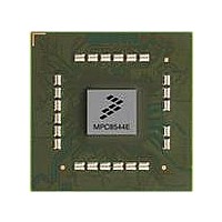
MPC8544DS Freescale Semiconductor, MPC8544DS Datasheet - Page 376

MPC8544DS
Manufacturer Part Number
MPC8544DS
Description
BOARD DEVELOPMENT SYSTEM 8544
Manufacturer
Freescale Semiconductor
Series
PowerQUICC III™r
Type
MPUr
Datasheets
1.MPC8544VTALF.pdf
(117 pages)
2.MPC8544VTALF.pdf
(2 pages)
3.MPC8544VTALF.pdf
(1340 pages)
4.MPC8544DS.pdf
(2 pages)
Specifications of MPC8544DS
Contents
Board
Processor To Be Evaluated
MPC8544E
Data Bus Width
32 bit
Interface Type
Ethernet, I2C
Operating Supply Voltage
- 0.3 V to + 1.1 V
Leaded Process Compatible
Yes
Peak Reflow Compatible (260 C)
Yes
Rohs Compliant
Yes
For Use With/related Products
MPC8544
For Use With
PPC8544EVTANG - EVAL MPC8544 783FCPBGA
Lead Free Status / RoHS Status
Lead free / RoHS Compliant
- MPC8544VTALF PDF datasheet
- MPC8544VTALF PDF datasheet #2
- MPC8544VTALF PDF datasheet #3
- MPC8544DS PDF datasheet #4
- Current page: 376 of 1340
- Download datasheet (12Mb)
DDR Memory Controller
9.5.3
The following section describes the commands and timings the controller uses when operating in DDR2
or DDR modes.
All read or write accesses to DDR SDRAM are performed by the DDR memory controller using JEDEC
standard DDR SDRAM interface commands. The SDRAM device samples command and address inputs
on rising edges of the memory clock; data is sampled using both the rising and falling edges of DQS. Data
read from the DDR SDRAM is also sampled on both edges of DQS.
The following DDR SDRAM interface commands (summarized in
controller. All actions for these commands are described from the perspective of the SDRAM device.
9-52
x 3
x 2
x 3
x 2
14
10
14
10
13
10
13
10
x
x
x
x
Row
•
•
•
Col
MRAS 13
MCAS
MRAS
MCAS
MRAS
MCAS
MRAS
MCAS
x
MBA
MBA
MBA
MBA
Row activate—Latches row address and initiates memory read of that row. Row data is latched in
SDRAM sense amplifiers and must be restored by a precharge command before another row
activate occurs.
Precharge—Restores data from the sense amplifiers to the appropriate row. Also initializes the
sense amplifiers in preparation for reading another row in the memory array, (performing another
activate command). Precharge must occur after read or write, if the row address changes on the
next open page mode access.
Read—Latches column address and transfers data from the selected sense amplifier to the output
buffer as determined by the column address. During each succeeding clock edge, additional data is
driven without additional read commands. The amount of data transferred is determined by the
burst size which defaults to 4.
msb
JEDEC Standard DDR SDRAM Interface Commands
4
MPC8544E PowerQUICC III Integrated Host Processor Family Reference Manual, Rev. 1
Table 9-45. Example of Address Multiplexing for 64-Bit Data Bus Interleaving
12 11 10 9
13 12 11 10 9
12 11 10
5
12 11 10 9
6
7
8
9
9 10 11 12 13 14 15 16 17 18 19 20 21 22 23 24 25 26 27 28 29 30 31 32 33–35
8
8
7
8
7
8
6
7
6
7
5
6
5
6
4
5
4
5
Between Four Banks
3
4
3
4
Address from Core Master
2
3
2
3
1
2
1
2
0
1 0
0
1
0
SEL
SEL
CS
CS
SEL
SEL
CS
CS
2 1 0
2
1 0
1
1
Table
0
0
9 8 7 6 5 4 3 2 1 0
9 8 7 6 5 4 3 2 1 0
9
9
9-46) are provided by the DDR
8
8
7
7
6
6
5
5
Freescale Semiconductor
4
4
3
3
2
2
1
1
0
0
lsb
Related parts for MPC8544DS
Image
Part Number
Description
Manufacturer
Datasheet
Request
R
Part Number:
Description:
Manufacturer:
Freescale Semiconductor, Inc
Datasheet:
Part Number:
Description:
Manufacturer:
Freescale Semiconductor, Inc
Datasheet:
Part Number:
Description:
Manufacturer:
Freescale Semiconductor, Inc
Datasheet:
Part Number:
Description:
Manufacturer:
Freescale Semiconductor, Inc
Datasheet:
Part Number:
Description:
Manufacturer:
Freescale Semiconductor, Inc
Datasheet:
Part Number:
Description:
Manufacturer:
Freescale Semiconductor, Inc
Datasheet:
Part Number:
Description:
Manufacturer:
Freescale Semiconductor, Inc
Datasheet:
Part Number:
Description:
Manufacturer:
Freescale Semiconductor, Inc
Datasheet:
Part Number:
Description:
Manufacturer:
Freescale Semiconductor, Inc
Datasheet:
Part Number:
Description:
Manufacturer:
Freescale Semiconductor, Inc
Datasheet:
Part Number:
Description:
Manufacturer:
Freescale Semiconductor, Inc
Datasheet:
Part Number:
Description:
Manufacturer:
Freescale Semiconductor, Inc
Datasheet:
Part Number:
Description:
Manufacturer:
Freescale Semiconductor, Inc
Datasheet:
Part Number:
Description:
Manufacturer:
Freescale Semiconductor, Inc
Datasheet:
Part Number:
Description:
Manufacturer:
Freescale Semiconductor, Inc
Datasheet:


