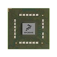
MPC8544DS Freescale Semiconductor, MPC8544DS Datasheet - Page 721

MPC8544DS
Manufacturer Part Number
MPC8544DS
Description
BOARD DEVELOPMENT SYSTEM 8544
Manufacturer
Freescale Semiconductor
Series
PowerQUICC III™r
Type
MPUr
Datasheets
1.MPC8544VTALF.pdf
(117 pages)
2.MPC8544VTALF.pdf
(2 pages)
3.MPC8544VTALF.pdf
(1340 pages)
4.MPC8544DS.pdf
(2 pages)
Specifications of MPC8544DS
Contents
Board
Processor To Be Evaluated
MPC8544E
Data Bus Width
32 bit
Interface Type
Ethernet, I2C
Operating Supply Voltage
- 0.3 V to + 1.1 V
Leaded Process Compatible
Yes
Peak Reflow Compatible (260 C)
Yes
Rohs Compliant
Yes
For Use With/related Products
MPC8544
For Use With
PPC8544EVTANG - EVAL MPC8544 783FCPBGA
Lead Free Status / RoHS Status
Lead free / RoHS Compliant
- MPC8544VTALF PDF datasheet
- MPC8544VTALF PDF datasheet #2
- MPC8544VTALF PDF datasheet #3
- MPC8544DS PDF datasheet #4
- Current page: 721 of 1340
- Download datasheet (12Mb)
14.5.6.1.3
As mentioned previously, to facilitate burst transfers the host’s local bus address lines can be connected in
a very specific way. First, the local bus A31 signal is not required, as the HDI16 registers are 16-bit word
addressed. Secondly, local bus LA[27] and LA[28] signals can be eliminated, so that the host side transmit
and receive registers wrap around the same four 16-bit word addresses.
For example, host transmit register 0 on the HDI16 peripheral (address 0x04) can be obtained by the host
by accessing any of the following memory mapped addresses: 0x20, 0x28, 0x30, or 0x38. This is critical
for burst accesses as the source or destination addresses increment after each 16-bit access to the interface
for all 16 transactions within that burst. By using the addressing as defined, if the first access is at 0x20,
the last will be at 0x3e but, more importantly, the four host Tx/Rx registers will have been looped around
four times.
14.5.6.1.4
The host UPM-controlled local bus and the HDI16 MSC8101 HDI16 host interface are both
programmable. Careful programming of the host chip select registers and UPM can meet the HDI16
MSC8101 host port timings.
On any bus access the critical timing for both read and write is typically around the data latch point. For
the UPM based read access, the host has the flexibility to latch data on a rising or falling LCLK edge. The
falling LCLK edge is used here to latch the HDI16 data into the host MSC8101 at its earliest convenience.
After the data is latched, appropriate HDI16 port data hold time is ensured before the data strobe (DS) and
chip select (CS1) are negated.
On a UPM write cycle, the critical action is in enveloping the DS assertion with CS asserted to ensure
proper write data hold time after latching by the HDI16 host port.
Special attention needs to be given to both the host read and write access strobe (DS) negation times (HDS
assert).
The HDI16 MSC8101 specifies some restrictions for consecutive register access, which results in a hold
off negation time for the read and write access strobes.
Freescale Semiconductor
•
•
Address lines—The address lines between the LBC and the HDI16 MSC8101 can either be
connected in a straightforward or a specific manner to enable burst transfers across the HDI16. The
connections are defined as follows and are described in more detail in the following sub-section:
— Either LA[27] or latched value of A25 -> HA0
— Either LA[28] or latched value of A26 -> HA1
— LA[29] -> HA2
— LA[30] -> HA3
Ground lines—In order to provide the best ground plane, it is highly advised that all grounds are
common and connected together.
MPC8544E PowerQUICC III Integrated Host Processor Family Reference Manual, Rev. 1
Supporting Burst Transfers
Host 60x Bus: HDI16 Peripheral Interface Hardware Timings
Local Bus Controller
14-101
Related parts for MPC8544DS
Image
Part Number
Description
Manufacturer
Datasheet
Request
R
Part Number:
Description:
Manufacturer:
Freescale Semiconductor, Inc
Datasheet:
Part Number:
Description:
Manufacturer:
Freescale Semiconductor, Inc
Datasheet:
Part Number:
Description:
Manufacturer:
Freescale Semiconductor, Inc
Datasheet:
Part Number:
Description:
Manufacturer:
Freescale Semiconductor, Inc
Datasheet:
Part Number:
Description:
Manufacturer:
Freescale Semiconductor, Inc
Datasheet:
Part Number:
Description:
Manufacturer:
Freescale Semiconductor, Inc
Datasheet:
Part Number:
Description:
Manufacturer:
Freescale Semiconductor, Inc
Datasheet:
Part Number:
Description:
Manufacturer:
Freescale Semiconductor, Inc
Datasheet:
Part Number:
Description:
Manufacturer:
Freescale Semiconductor, Inc
Datasheet:
Part Number:
Description:
Manufacturer:
Freescale Semiconductor, Inc
Datasheet:
Part Number:
Description:
Manufacturer:
Freescale Semiconductor, Inc
Datasheet:
Part Number:
Description:
Manufacturer:
Freescale Semiconductor, Inc
Datasheet:
Part Number:
Description:
Manufacturer:
Freescale Semiconductor, Inc
Datasheet:
Part Number:
Description:
Manufacturer:
Freescale Semiconductor, Inc
Datasheet:
Part Number:
Description:
Manufacturer:
Freescale Semiconductor, Inc
Datasheet:


