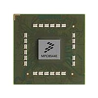
MPC8544DS Freescale Semiconductor, MPC8544DS Datasheet - Page 327

MPC8544DS
Manufacturer Part Number
MPC8544DS
Description
BOARD DEVELOPMENT SYSTEM 8544
Manufacturer
Freescale Semiconductor
Series
PowerQUICC III™r
Type
MPUr
Datasheets
1.MPC8544VTALF.pdf
(117 pages)
2.MPC8544VTALF.pdf
(2 pages)
3.MPC8544VTALF.pdf
(1340 pages)
4.MPC8544DS.pdf
(2 pages)
Specifications of MPC8544DS
Contents
Board
Processor To Be Evaluated
MPC8544E
Data Bus Width
32 bit
Interface Type
Ethernet, I2C
Operating Supply Voltage
- 0.3 V to + 1.1 V
Leaded Process Compatible
Yes
Peak Reflow Compatible (260 C)
Yes
Rohs Compliant
Yes
For Use With/related Products
MPC8544
For Use With
PPC8544EVTANG - EVAL MPC8544 783FCPBGA
Lead Free Status / RoHS Status
Lead free / RoHS Compliant
- MPC8544VTALF PDF datasheet
- MPC8544VTALF PDF datasheet #2
- MPC8544VTALF PDF datasheet #3
- MPC8544DS PDF datasheet #4
- Current page: 327 of 1340
- Download datasheet (12Mb)
9.2.1
The DDR memory controller supports the following modes:
9.3
This section provides descriptions of the DDR memory controller’s external signals. It describes each
signal’s behavior when the signal is asserted or negated and when the signal is an input or an output.
9.3.1
Memory controller signals are grouped as follows:
Table 9-1
specification has a pinout diagram showing pin numbers. It also lists all electrical and mechanical
specifications.
Freescale Semiconductor
•
•
•
•
•
•
•
•
•
Automatic DRAM data initialization
Support for up to eight posted refreshes
Memory controller clock frequency of two times the SDRAM clock with support for sleep power
management
Support for error injection
Dynamic power management mode. The DDR memory controller can reduce power consumption
by negating the SDRAM CKE signal when no transactions are pending to the SDRAM.
Auto-precharge mode. Clearing DDR_SDRAM_INTERVAL[BSTOPRE] causes the memory
controller to issue an auto-precharge command with every read or write transaction.
Auto-precharge mode can be enabled for separate chip selects by setting
CSn_CONFIG[AP_n_EN].
Memory interface signals
Clock signals
Debug signals
External Signal Descriptions
shows how DDR memory controller external signals are grouped. The device hardware
Modes of Operation
Signals Overview
MPC8544E PowerQUICC III Integrated Host Processor Family Reference Manual, Rev. 1
MDQ[0:63]
MDQS[0:8]
MDQS[0:8]
MECC[0:7]
MBA[2:0]
MA[15:0]
MCAS
Name
Table 9-1. DDR Memory Interface Signal Summary
Data bus
Data strobes
Complement data strobes
Error checking and correcting
Column address strobe
Address bus
Logical bank address
Function/Description
All zeros
All zeros
All zeros
All zeros
All zeros
All ones
Reset
One
Pins
64
16
9
9
8
1
3
I/O
I/O
I/O
I/O
I/O
O
O
O
DDR Memory Controller
9-3
Related parts for MPC8544DS
Image
Part Number
Description
Manufacturer
Datasheet
Request
R
Part Number:
Description:
Manufacturer:
Freescale Semiconductor, Inc
Datasheet:
Part Number:
Description:
Manufacturer:
Freescale Semiconductor, Inc
Datasheet:
Part Number:
Description:
Manufacturer:
Freescale Semiconductor, Inc
Datasheet:
Part Number:
Description:
Manufacturer:
Freescale Semiconductor, Inc
Datasheet:
Part Number:
Description:
Manufacturer:
Freescale Semiconductor, Inc
Datasheet:
Part Number:
Description:
Manufacturer:
Freescale Semiconductor, Inc
Datasheet:
Part Number:
Description:
Manufacturer:
Freescale Semiconductor, Inc
Datasheet:
Part Number:
Description:
Manufacturer:
Freescale Semiconductor, Inc
Datasheet:
Part Number:
Description:
Manufacturer:
Freescale Semiconductor, Inc
Datasheet:
Part Number:
Description:
Manufacturer:
Freescale Semiconductor, Inc
Datasheet:
Part Number:
Description:
Manufacturer:
Freescale Semiconductor, Inc
Datasheet:
Part Number:
Description:
Manufacturer:
Freescale Semiconductor, Inc
Datasheet:
Part Number:
Description:
Manufacturer:
Freescale Semiconductor, Inc
Datasheet:
Part Number:
Description:
Manufacturer:
Freescale Semiconductor, Inc
Datasheet:
Part Number:
Description:
Manufacturer:
Freescale Semiconductor, Inc
Datasheet:


