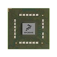
MPC8544DS Freescale Semiconductor, MPC8544DS Datasheet - Page 456

MPC8544DS
Manufacturer Part Number
MPC8544DS
Description
BOARD DEVELOPMENT SYSTEM 8544
Manufacturer
Freescale Semiconductor
Series
PowerQUICC III™r
Type
MPUr
Datasheets
1.MPC8544VTALF.pdf
(117 pages)
2.MPC8544VTALF.pdf
(2 pages)
3.MPC8544VTALF.pdf
(1340 pages)
4.MPC8544DS.pdf
(2 pages)
Specifications of MPC8544DS
Contents
Board
Processor To Be Evaluated
MPC8544E
Data Bus Width
32 bit
Interface Type
Ethernet, I2C
Operating Supply Voltage
- 0.3 V to + 1.1 V
Leaded Process Compatible
Yes
Peak Reflow Compatible (260 C)
Yes
Rohs Compliant
Yes
For Use With/related Products
MPC8544
For Use With
PPC8544EVTANG - EVAL MPC8544 783FCPBGA
Lead Free Status / RoHS Status
Lead free / RoHS Compliant
- MPC8544VTALF PDF datasheet
- MPC8544VTALF PDF datasheet #2
- MPC8544VTALF PDF datasheet #3
- MPC8544DS PDF datasheet #4
- Current page: 456 of 1340
- Download datasheet (12Mb)
I
11.1.1
The two-wire I
bus allows the connection of additional devices to the bus for expansion and system development. The bus
includes collision detection and arbitration that prevent data corruption if two or more masters attempt to
control the bus simultaneously.
11.1.2
The I
11.1.3
The I
11-2
2
C Interfaces
•
•
•
•
•
•
•
•
•
•
•
•
•
•
2
2
C interface includes the following features:
C units on this device can operate in one of the following modes:
Two-wire interface
Multiple-master operation
Arbitration lost interrupt with automatic mode switching from master to slave
Calling address identification interrupt
START and STOP signal generation/detection
Acknowledge bit generation/detection
Bus busy detection
Software-programmable clock frequency
Software-selectable acknowledge bit
On-chip filtering for spikes on the bus
Master mode—The I
address. The I
Slave mode—The I
START condition from a non-I
Interrupt-driven byte-to-byte data transfer—When successful slave addressing is achieved (and
SCL returns to zero), the data transfer can proceed on a byte-to-byte basis in the direction specified
by the R/W bit sent by the calling master. Each byte of data must be followed by an acknowledge
bit, which is signaled from the receiving device. Several bytes can be transferred during a data
transfer session.
Boot sequencer mode—This mode can be used to initialize the configuration registers in the device
after the I
disabled as a default, but this mode can be selected with the cfg_boot_seq[0:1] power-on reset
(POR) configuration signals that are located on the LGPL3 and LGPL5 signals.
Overview
Features
Modes of Operation
MPC8544E PowerQUICC III Integrated Host Processor Family Reference Manual, Rev. 1
2
C bus minimizes interconnections between devices. The synchronous, multiple-master I
2
C1 module is initialized. Note that the device powers up with boot sequencer mode
2
C cannot be a master and a slave simultaneously.
2
2
C is not the driver of the SDA line. The module must be enabled before a
C is the driver of the SDA line. It cannot use its own slave address as a calling
2
C master is detected.
Freescale Semiconductor
2
C
Related parts for MPC8544DS
Image
Part Number
Description
Manufacturer
Datasheet
Request
R
Part Number:
Description:
Manufacturer:
Freescale Semiconductor, Inc
Datasheet:
Part Number:
Description:
Manufacturer:
Freescale Semiconductor, Inc
Datasheet:
Part Number:
Description:
Manufacturer:
Freescale Semiconductor, Inc
Datasheet:
Part Number:
Description:
Manufacturer:
Freescale Semiconductor, Inc
Datasheet:
Part Number:
Description:
Manufacturer:
Freescale Semiconductor, Inc
Datasheet:
Part Number:
Description:
Manufacturer:
Freescale Semiconductor, Inc
Datasheet:
Part Number:
Description:
Manufacturer:
Freescale Semiconductor, Inc
Datasheet:
Part Number:
Description:
Manufacturer:
Freescale Semiconductor, Inc
Datasheet:
Part Number:
Description:
Manufacturer:
Freescale Semiconductor, Inc
Datasheet:
Part Number:
Description:
Manufacturer:
Freescale Semiconductor, Inc
Datasheet:
Part Number:
Description:
Manufacturer:
Freescale Semiconductor, Inc
Datasheet:
Part Number:
Description:
Manufacturer:
Freescale Semiconductor, Inc
Datasheet:
Part Number:
Description:
Manufacturer:
Freescale Semiconductor, Inc
Datasheet:
Part Number:
Description:
Manufacturer:
Freescale Semiconductor, Inc
Datasheet:
Part Number:
Description:
Manufacturer:
Freescale Semiconductor, Inc
Datasheet:


