ATSAM3U-EK Atmel, ATSAM3U-EK Datasheet - Page 113
ATSAM3U-EK
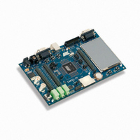
Manufacturer Part Number
ATSAM3U-EK
Description
KIT EVAL FOR AT91SAM3U CORTEX
Manufacturer
Atmel
Type
MCUr
Datasheets
1.ATSAM3U-EK.pdf
(2 pages)
2.ATSAM3U-EK.pdf
(61 pages)
3.ATSAM3U-EK.pdf
(1171 pages)
4.ATSAM3U-EK.pdf
(53 pages)
Specifications of ATSAM3U-EK
Contents
Board
Processor To Be Evaluated
SAM3U
Data Bus Width
32 bit
Interface Type
RS-232, USB
Operating Supply Voltage
3 V
Silicon Manufacturer
Atmel
Core Architecture
ARM
Core Sub-architecture
Cortex - M3
Silicon Core Number
SAM3U4E
Silicon Family Name
SAM3U
Kit Contents
Board CD Docs
Rohs Compliant
Yes
For Use With/related Products
AT91SAM3U
Lead Free Status / RoHS Status
Lead free / RoHS Compliant
Available stocks
Company
Part Number
Manufacturer
Quantity
Price
Company:

Part Number:
ATSAM3U-EK
Manufacturer:
Atmel
Quantity:
10


13.11.6
13.11.6.1
13.11.6.2
6430D–ATARM–25-Mar-11
LDM and STM
Syntax
Operation
Load and Store Multiple registers.
where:
op
addr_mode
cond
Rn
!
reglist
contain register ranges. It must be comma separated if it contains more than one register or reg-
ister range, see
LDM and LDMFD are synonyms for LDMIA. LDMFD refers to its use for popping data from Full
Descending stacks.
LDMEA is a synonym for LDMDB, and refers to its use for popping data from Empty Ascending
stacks.
STM and STMEA are synonyms for STMIA. STMEA refers to its use for pushing data onto
Empty Ascending stacks.
STMFD is s synonym for STMDB, and refers to its use for pushing data onto Full Descending
stacks
LDM instructions load the registers in reglist with word values from memory addresses based on
Rn.
STM instructions store the word values in the registers in reglist to memory addresses based on
Rn.
For LDM, LDMIA, LDMFD, STM, STMIA, and STMEA the memory addresses used for the
accesses are at 4-byte intervals ranging from Rn to Rn + 4 * (n-1), where n is the number of reg-
isters in reglist. The accesses happens in order of increasing register numbers, with the lowest
numbered register using the lowest memory address and the highest number register using the
highest memory address. If the writeback suffix is specified, the value of Rn + 4 * (n-1) is written
back to Rn.
For LDMDB, LDMEA, STMDB, and STMFD the memory addresses used for the accesses are at
4-byte intervals ranging from Rn to Rn - 4 * (n-1), where n is the number of registers in reglist.
op{addr_mode}{cond} Rn{!}, reglist
LDM
STM
IA
DB
If ! is present the final address, that is loaded from or stored to, is written back into Rn.
is one of:
Load Multiple registers.
Store Multiple registers.
is any one of the following:
Increment address After each access. This is the default.
Decrement address Before each access.
is an optional condition code, see
is the register on which the memory addresses are based.
is an optional writeback suffix.
is a list of one or more registers to be loaded or stored, enclosed in braces. It can
“Examples” on page
114.
“Conditional execution” on page
SAM3U Series
100.
113
Related parts for ATSAM3U-EK
Image
Part Number
Description
Manufacturer
Datasheet
Request
R

Part Number:
Description:
AT91 ARM Thumb-based Microcontrollers
Manufacturer:
ATMEL [ATMEL Corporation]
Datasheet:

Part Number:
Description:
DEV KIT FOR AVR/AVR32
Manufacturer:
Atmel
Datasheet:

Part Number:
Description:
INTERVAL AND WIPE/WASH WIPER CONTROL IC WITH DELAY
Manufacturer:
ATMEL Corporation
Datasheet:
Part Number:
Description:
Low-Voltage Voice-Switched IC for Hands-Free Operation
Manufacturer:
ATMEL Corporation
Datasheet:
Part Number:
Description:
MONOLITHIC INTEGRATED FEATUREPHONE CIRCUIT
Manufacturer:
ATMEL Corporation
Datasheet:
Part Number:
Description:
AM-FM Receiver IC U4255BM-M
Manufacturer:
ATMEL Corporation
Datasheet:
Part Number:
Description:
Monolithic Integrated Feature Phone Circuit
Manufacturer:
ATMEL Corporation
Datasheet:
Part Number:
Description:
Multistandard Video-IF and Quasi Parallel Sound Processing
Manufacturer:
ATMEL Corporation
Datasheet:
Part Number:
Description:
High-performance EE PLD
Manufacturer:
ATMEL Corporation
Datasheet:
Part Number:
Description:
8-bit Flash Microcontroller
Manufacturer:
ATMEL Corporation
Datasheet:
Part Number:
Description:
2-Wire Serial EEPROM
Manufacturer:
ATMEL Corporation
Datasheet: