ATSAM3U-EK Atmel, ATSAM3U-EK Datasheet - Page 313
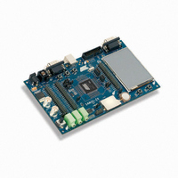
ATSAM3U-EK
Manufacturer Part Number
ATSAM3U-EK
Description
KIT EVAL FOR AT91SAM3U CORTEX
Manufacturer
Atmel
Type
MCUr
Datasheets
1.ATSAM3U-EK.pdf
(2 pages)
2.ATSAM3U-EK.pdf
(61 pages)
3.ATSAM3U-EK.pdf
(1171 pages)
4.ATSAM3U-EK.pdf
(53 pages)
Specifications of ATSAM3U-EK
Contents
Board
Processor To Be Evaluated
SAM3U
Data Bus Width
32 bit
Interface Type
RS-232, USB
Operating Supply Voltage
3 V
Silicon Manufacturer
Atmel
Core Architecture
ARM
Core Sub-architecture
Cortex - M3
Silicon Core Number
SAM3U4E
Silicon Family Name
SAM3U
Kit Contents
Board CD Docs
Rohs Compliant
Yes
For Use With/related Products
AT91SAM3U
Lead Free Status / RoHS Status
Lead free / RoHS Compliant
Available stocks
Company
Part Number
Manufacturer
Quantity
Price
Company:

Part Number:
ATSAM3U-EK
Manufacturer:
Atmel
Quantity:
10


Table 21-3.
21.3.3.2
6430D–ATARM–25-Mar-11
Symbol
FL_ID
FL_SIZE
FL_PAGE_SIZE
FL_NB_PLANE
FL_PLANE[0]
...
FL_PLANE[FL_NB_PLANE-1]
FL_NB_LOCK
FL_LOCK[0]
...
Write Commands
Flash Descriptor Definition
ations to the EEFC_FRR register are done after the last word of the descriptor has been
returned, then the EEFC_FRR register value is 0 until the next valid command.
Several commands can be used to program the Flash.
Flash technology requires that an erase is done before programming. The full memory plane can
be erased at the same time, or several pages can be erased at the same time (refer to
21.3.3.3 ”Erase
using EWP or EWPL commands.
After programming, the page (the whole lock region) can be locked to prevent miscellaneous
write or erase sequences. The lock bit can be automatically set after page programming using
WPL or EWPL commands.
Data to be written are stored in an internal latch buffer. The size of the latch buffer corresponds
to the page size. The latch buffer wraps around within the internal memory area address space
and is repeated as many times as the number of pages within this address space.
Note:
Write operations are performed in a number of wait states equal to the number of wait states for
read operations.
Data are written to the latch buffer before the programming command is written to the Flash
Command Register EEFC_FCR. The sequence is as follows:
Two errors can be detected in the EEFC_FSR register after a programming sequence:
• Write the full page, at any page address, within the internal memory area address space.
• Programming starts as soon as the page number and the programming command are written
• When programming is completed, the FRDY bit in the Flash Programming Status Register
to the Flash Command Register. The FRDY bit in the Flash Programming Status Register
(EEFC_FSR) is automatically cleared.
(EEFC_FSR) rises. If an interrupt has been enabled by setting the bit FRDY in EEFC_FMR,
the corresponding interrupt line of the NVIC is activated.
Writing of 8-bit and 16-bit data is not allowed and may lead to unpredictable data corruption.
Word Index
0
1
2
3
4
4 + FL_NB_PLANE - 1
4 + FL_NB_PLANE + 1
4 + FL_NB_PLANE
Commands”). Also, a page erase can be automatically done before a page write
Description
Flash Interface Description
Flash size in bytes
Page size in bytes
Number of planes.
Number of bytes in the first plane.
Number of bytes in the last plane.
Number of lock bits. A bit is associated
with a lock region. A lock bit is used to
prevent write or erase operations in the
lock region.
Number of bytes in the first lock region.
SAM3U Series
Section
313
Related parts for ATSAM3U-EK
Image
Part Number
Description
Manufacturer
Datasheet
Request
R

Part Number:
Description:
AT91 ARM Thumb-based Microcontrollers
Manufacturer:
ATMEL [ATMEL Corporation]
Datasheet:

Part Number:
Description:
DEV KIT FOR AVR/AVR32
Manufacturer:
Atmel
Datasheet:

Part Number:
Description:
INTERVAL AND WIPE/WASH WIPER CONTROL IC WITH DELAY
Manufacturer:
ATMEL Corporation
Datasheet:
Part Number:
Description:
Low-Voltage Voice-Switched IC for Hands-Free Operation
Manufacturer:
ATMEL Corporation
Datasheet:
Part Number:
Description:
MONOLITHIC INTEGRATED FEATUREPHONE CIRCUIT
Manufacturer:
ATMEL Corporation
Datasheet:
Part Number:
Description:
AM-FM Receiver IC U4255BM-M
Manufacturer:
ATMEL Corporation
Datasheet:
Part Number:
Description:
Monolithic Integrated Feature Phone Circuit
Manufacturer:
ATMEL Corporation
Datasheet:
Part Number:
Description:
Multistandard Video-IF and Quasi Parallel Sound Processing
Manufacturer:
ATMEL Corporation
Datasheet:
Part Number:
Description:
High-performance EE PLD
Manufacturer:
ATMEL Corporation
Datasheet:
Part Number:
Description:
8-bit Flash Microcontroller
Manufacturer:
ATMEL Corporation
Datasheet:
Part Number:
Description:
2-Wire Serial EEPROM
Manufacturer:
ATMEL Corporation
Datasheet: