ATSAM3U-EK Atmel, ATSAM3U-EK Datasheet - Page 34
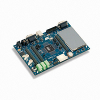
ATSAM3U-EK
Manufacturer Part Number
ATSAM3U-EK
Description
KIT EVAL FOR AT91SAM3U CORTEX
Manufacturer
Atmel
Type
MCUr
Datasheets
1.ATSAM3U-EK.pdf
(2 pages)
2.ATSAM3U-EK.pdf
(61 pages)
3.ATSAM3U-EK.pdf
(1171 pages)
4.ATSAM3U-EK.pdf
(53 pages)
Specifications of ATSAM3U-EK
Contents
Board
Processor To Be Evaluated
SAM3U
Data Bus Width
32 bit
Interface Type
RS-232, USB
Operating Supply Voltage
3 V
Silicon Manufacturer
Atmel
Core Architecture
ARM
Core Sub-architecture
Cortex - M3
Silicon Core Number
SAM3U4E
Silicon Family Name
SAM3U
Kit Contents
Board CD Docs
Rohs Compliant
Yes
For Use With/related Products
AT91SAM3U
Lead Free Status / RoHS Status
Lead free / RoHS Compliant
Available stocks
Company
Part Number
Manufacturer
Quantity
Price
Company:

Part Number:
ATSAM3U-EK
Manufacturer:
Atmel
Quantity:
10


9.1.4
9.2
9.2.1
9.2.2
9.2.3
34
External Memories
SAM3U Series
Boot Strategies
Static Memory Controller
NAND Flash Controller
NAND Flash Error Corrected Code Controller
The system always boots at address 0x0. To ensure a maximum boot possibilities the memory
layout can be changed via GPNVM.
A general purpose NVM (GPNVM1) bit is used to boot either on the ROM (default) or from the
Flash.
The GPNVM bit can be cleared or set respectively through the commands “Clear General-pur-
pose NVM Bit” and “Set General-purpose NVM Bit” of the EEFC User Interface.
Setting the GPNVM Bit 1 selects the boot from the Flash, clearing it selects the boot from the
ROM. Asserting ERASE clears the GPNVM Bit 1 and thus selects the boot from the ROM by
default.
GPNVM2 enables to select if Flash 0 or Flash 1 is used for the boot. Setting the GPNVM2 bit
selects the boot from Flash 1, clearing it selects the boot from Flash 0.
The SAM3U offers an interface to a wide range of external memories and to any parallel
peripheral.
• 8- or 16- bit Data Bus
• Up to 24-bit Address Bus (up to 16 MBytes linear per chip select)
• Up to 4 chips selects, Configurable Assignment
• Multiple Access Modes supported
• Multiple device adaptability
• Multiple Wait State Management
• Slow Clock mode supported
• Handles automatic Read/Write transfer through 4224 bytes SRAM buffer
• DMA support
• Supports SLC NAND Flash technology
• Programmable timing on a per chip select basis
• Programmable Flash Data width 8-bit or 16-bit
• Integrated in the NAND Flash Controller
• Single bit error correction and 2-bit Random detection.
• Automatic Hamming Code Calculation while writing
• Automatic Hamming Code Calculation while reading
– Byte Write or Byte Select Lines
– Control signals programmable setup, pulse and hold time for each Memory Bank
– Programmable Wait State Generation
– External Wait Request
– Programmable Data Float Time
– ECC value available in a register
6430D–ATARM–25-Mar-11
Related parts for ATSAM3U-EK
Image
Part Number
Description
Manufacturer
Datasheet
Request
R

Part Number:
Description:
AT91 ARM Thumb-based Microcontrollers
Manufacturer:
ATMEL [ATMEL Corporation]
Datasheet:

Part Number:
Description:
DEV KIT FOR AVR/AVR32
Manufacturer:
Atmel
Datasheet:

Part Number:
Description:
INTERVAL AND WIPE/WASH WIPER CONTROL IC WITH DELAY
Manufacturer:
ATMEL Corporation
Datasheet:
Part Number:
Description:
Low-Voltage Voice-Switched IC for Hands-Free Operation
Manufacturer:
ATMEL Corporation
Datasheet:
Part Number:
Description:
MONOLITHIC INTEGRATED FEATUREPHONE CIRCUIT
Manufacturer:
ATMEL Corporation
Datasheet:
Part Number:
Description:
AM-FM Receiver IC U4255BM-M
Manufacturer:
ATMEL Corporation
Datasheet:
Part Number:
Description:
Monolithic Integrated Feature Phone Circuit
Manufacturer:
ATMEL Corporation
Datasheet:
Part Number:
Description:
Multistandard Video-IF and Quasi Parallel Sound Processing
Manufacturer:
ATMEL Corporation
Datasheet:
Part Number:
Description:
High-performance EE PLD
Manufacturer:
ATMEL Corporation
Datasheet:
Part Number:
Description:
8-bit Flash Microcontroller
Manufacturer:
ATMEL Corporation
Datasheet:
Part Number:
Description:
2-Wire Serial EEPROM
Manufacturer:
ATMEL Corporation
Datasheet: