ATSAM3U-EK Atmel, ATSAM3U-EK Datasheet - Page 364
ATSAM3U-EK
Manufacturer Part Number
ATSAM3U-EK
Description
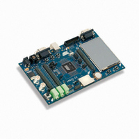
KIT EVAL FOR AT91SAM3U CORTEX
Manufacturer
Atmel
Type
MCUr
Datasheets
1.ATSAM3U-EK.pdf
(2 pages)
2.ATSAM3U-EK.pdf
(61 pages)
3.ATSAM3U-EK.pdf
(1171 pages)
4.ATSAM3U-EK.pdf
(53 pages)
Specifications of ATSAM3U-EK
Contents
Board
Processor To Be Evaluated
SAM3U
Data Bus Width
32 bit
Interface Type
RS-232, USB
Operating Supply Voltage
3 V
Silicon Manufacturer
Atmel
Core Architecture
ARM
Core Sub-architecture
Cortex - M3
Silicon Core Number
SAM3U4E
Silicon Family Name
SAM3U
Kit Contents
Board CD Docs
Rohs Compliant
Yes
For Use With/related Products
AT91SAM3U
Lead Free Status / RoHS Status
Lead free / RoHS Compliant
Available stocks
Company
Part Number
Manufacturer
Quantity
Price
Company:

Part Number:
ATSAM3U-EK
Manufacturer:
Atmel
Quantity:
10


25.10.3.3
25.10.4
25.10.4.1
Figure 25-11. WRITE_MODE = 1. The write operation is controlled by NWE
25.10.4.2
364
364
SAM3U Series
SAM3U Series
Write Mode
Write Cycle
Write is Controlled by NWE (WRITE_MODE = 1)
Write is Controlled by NCS (WRITE_MODE = 0)
NWR0, NWR1
NBS0, NBS1,
A0, A1
D[15:0]
A [23:2]
NWE,
MCK
NCS
The write cycle time is defined as the total duration of the write cycle, that is, from the time where
address is set on the address bus to the point where address may change. The total write cycle
time is equal to:
NWE_CYCLE = NWE_SETUP + NWE_PULSE + NWE_HOLD
= NCS_WR_SETUP + NCS_WR_PULSE + NCS_WR_HOLD
All NWE and NCS (write) timings are defined separately for each chip select as an integer num-
ber of Master Clock cycles. To ensure that the NWE and NCS timings are coherent, the user
must define the total write cycle instead of the hold timing. This implicitly defines the NWE hold
time and NCS (write) hold times as:
NWE_HOLD = NWE_CYCLE - NWE_SETUP - NWE_PULSE
NCS_WR_HOLD = NWE_CYCLE - NCS_WR_SETUP - NCS_WR_PULSE
The WRITE_MODE parameter in the SMC_MODE register of the corresponding chip select indi-
cates which signal controls the write operation.
Figure 25-11
put on the bus during the pulse and hold steps of the NWE signal. The internal data buffers are
turned out after the NWE_SETUP time, and until the end of the write cycle, regardless of the
programmed waveform on NCS.
Figure 25-12
put on the bus during the pulse and hold steps of the NCS signal. The internal data buffers are
turned out after the NCS_WR_SETUP time, and until the end of the write cycle, regardless of
the programmed waveform on NWE.
shows the waveforms of a write operation with WRITE_MODE set to 1. The data is
shows the waveforms of a write operation with WRITE_MODE set to 0. The data is
6430D–ATARM–25-Mar-11
6430D–ATARM–25-Mar-11
Related parts for ATSAM3U-EK
Image
Part Number
Description
Manufacturer
Datasheet
Request
R

Part Number:
Description:
AT91 ARM Thumb-based Microcontrollers
Manufacturer:
ATMEL [ATMEL Corporation]
Datasheet:

Part Number:
Description:
DEV KIT FOR AVR/AVR32
Manufacturer:
Atmel
Datasheet:

Part Number:
Description:
INTERVAL AND WIPE/WASH WIPER CONTROL IC WITH DELAY
Manufacturer:
ATMEL Corporation
Datasheet:
Part Number:
Description:
Low-Voltage Voice-Switched IC for Hands-Free Operation
Manufacturer:
ATMEL Corporation
Datasheet:
Part Number:
Description:
MONOLITHIC INTEGRATED FEATUREPHONE CIRCUIT
Manufacturer:
ATMEL Corporation
Datasheet:
Part Number:
Description:
AM-FM Receiver IC U4255BM-M
Manufacturer:
ATMEL Corporation
Datasheet:
Part Number:
Description:
Monolithic Integrated Feature Phone Circuit
Manufacturer:
ATMEL Corporation
Datasheet:
Part Number:
Description:
Multistandard Video-IF and Quasi Parallel Sound Processing
Manufacturer:
ATMEL Corporation
Datasheet:
Part Number:
Description:
High-performance EE PLD
Manufacturer:
ATMEL Corporation
Datasheet:
Part Number:
Description:
8-bit Flash Microcontroller
Manufacturer:
ATMEL Corporation
Datasheet:
Part Number:
Description:
2-Wire Serial EEPROM
Manufacturer:
ATMEL Corporation
Datasheet: