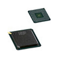
PNX1500E NXP Semiconductors, PNX1500E Datasheet - Page 115

PNX1500E
Manufacturer Part Number
PNX1500E
Description
Manufacturer
NXP Semiconductors
Datasheet
1.PNX1500E.pdf
(828 pages)
Specifications of PNX1500E
Lead Free Status / Rohs Status
Not Compliant
Available stocks
Company
Part Number
Manufacturer
Quantity
Price
Company:
Part Number:
PNX1500E
Manufacturer:
NORTEL
Quantity:
1 000
- Current page: 115 of 828
- Download datasheet (4Mb)
NXP Semiconductors
Volume 1 of 1
3. System Principles
PNX15XX_PNX952X_SER_N_4
Product data sheet
3.1 Module ID
3.2 Powerdown bit
Other than the PCI module, only the TM3260 CPU can emit requests to the PCI bus,
i.e. none of the other PNX15xx/952x Series modules can do so.
Only the TM3260 CPU and external PCI master can request MMIO reads or writes.
The XIO aperture can only be accessed by the TM3260 CPU.
The system resources module is like any other module composing the PNX15xx/
952x Series system. Like the other modules it has a Module ID MMIO register as well
as powerdown MMIO register.
The module ID MMIO register is used to differentiate between the different modules
of the system and different revisions of the same module. For all the modules the
MMIO content is composed of:
This is a read only register. See
Major powerdown saving is achieved by turning off the clock that feeds the module.
The safe procedure to turn off the clock of a module is to write a ‘1’ to the powerdown
bit located in each module of the system before turning off its clock (whenever it is
possible). Similarly when powering the module back up, the clock should be turned
on before the powerdown bit is flipped back to ‘0’. When the powerdown bit is
activated the module will no longer respond to MMIO read or writes other than
transactions targeting the powerdown bit.
Most of the PNX15xx/952x Series modules need two different clocks to operate. The
streaming clock, e.g. the video pixel clock for QVCP, and the MMIO or DCS clock.
Only the streaming clock should be turned off. Therefore, locally some modules may
do extra clock gating on the DCS clock when the powerdown bit is turned on.
For the system module there is no streaming clock to turn off. Details on the MMIO
register layout is available in the next
•
•
•
An unique 16-bit Module ID. This ID is only changed if the functionality of the
Module changes significantly. Module IDs 0 and 1 are reserved.
An 8-bit revision ID composed of a 4-bit MAJOR_REV ID and a 4-bit
MINOR_REV ID. MAJOR_REV ID is changed upon changing functionality of the
module, while the MINOR_REV ID is changed in case of bug fixing or non
functional fixes like yield improvements.
An 8-bit value to code the range of recognized MMIO addresses by the module.
This aperture size allows the module to claim one offset region of the MMIO
Aperture. The offset region or local aperture is defined by the following formula,
(N + 1) * 4 Kilobytes, where N is the 8-bit code stored in the module ID register.
Rev. 4.0 — 03 December 2007
Section 3.3
Section
Chapter 3: System On Chip Resources
for details on the system module ID.
3.3.
PNX15xx/952x Series
© NXP B.V. 2007. All rights reserved.
3-115
Related parts for PNX1500E
Image
Part Number
Description
Manufacturer
Datasheet
Request
R
Part Number:
Description:
NXP Semiconductors designed the LPC2420/2460 microcontroller around a 16-bit/32-bitARM7TDMI-S CPU core with real-time debug interfaces that include both JTAG andembedded trace
Manufacturer:
NXP Semiconductors
Datasheet:

Part Number:
Description:
NXP Semiconductors designed the LPC2458 microcontroller around a 16-bit/32-bitARM7TDMI-S CPU core with real-time debug interfaces that include both JTAG andembedded trace
Manufacturer:
NXP Semiconductors
Datasheet:
Part Number:
Description:
NXP Semiconductors designed the LPC2468 microcontroller around a 16-bit/32-bitARM7TDMI-S CPU core with real-time debug interfaces that include both JTAG andembedded trace
Manufacturer:
NXP Semiconductors
Datasheet:
Part Number:
Description:
NXP Semiconductors designed the LPC2470 microcontroller, powered by theARM7TDMI-S core, to be a highly integrated microcontroller for a wide range ofapplications that require advanced communications and high quality graphic displays
Manufacturer:
NXP Semiconductors
Datasheet:
Part Number:
Description:
NXP Semiconductors designed the LPC2478 microcontroller, powered by theARM7TDMI-S core, to be a highly integrated microcontroller for a wide range ofapplications that require advanced communications and high quality graphic displays
Manufacturer:
NXP Semiconductors
Datasheet:
Part Number:
Description:
The Philips Semiconductors XA (eXtended Architecture) family of 16-bit single-chip microcontrollers is powerful enough to easily handle the requirements of high performance embedded applications, yet inexpensive enough to compete in the market for hi
Manufacturer:
NXP Semiconductors
Datasheet:
Part Number:
Description:
The XA-S3 device is a member of Philips Semiconductors? XA(eXtended Architecture) family of high performance 16-bitsingle-chip microcontrollers
Manufacturer:
NXP Semiconductors
Datasheet:

Part Number:
Description:
The NXP BlueStreak LH75401/LH75411 family consists of two low-cost 16/32-bit System-on-Chip (SoC) devices
Manufacturer:
NXP Semiconductors
Datasheet:

Part Number:
Description:
The NXP LPC3130/3131 combine an 180 MHz ARM926EJ-S CPU core, high-speed USB2
Manufacturer:
NXP Semiconductors
Datasheet:

Part Number:
Description:
The NXP LPC3141 combine a 270 MHz ARM926EJ-S CPU core, High-speed USB 2
Manufacturer:
NXP Semiconductors

Part Number:
Description:
The NXP LPC3143 combine a 270 MHz ARM926EJ-S CPU core, High-speed USB 2
Manufacturer:
NXP Semiconductors

Part Number:
Description:
The NXP LPC3152 combines an 180 MHz ARM926EJ-S CPU core, High-speed USB 2
Manufacturer:
NXP Semiconductors

Part Number:
Description:
The NXP LPC3154 combines an 180 MHz ARM926EJ-S CPU core, High-speed USB 2
Manufacturer:
NXP Semiconductors

Part Number:
Description:
Standard level N-channel enhancement mode Field-Effect Transistor (FET) in a plastic package using NXP High-Performance Automotive (HPA) TrenchMOS technology
Manufacturer:
NXP Semiconductors
Datasheet:


