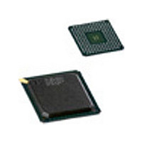
PNX1500E NXP Semiconductors, PNX1500E Datasheet - Page 541

PNX1500E
Manufacturer Part Number
PNX1500E
Description
Manufacturer
NXP Semiconductors
Datasheet
1.PNX1500E.pdf
(828 pages)
Specifications of PNX1500E
Lead Free Status / Rohs Status
Not Compliant
Available stocks
Company
Part Number
Manufacturer
Quantity
Price
Company:
Part Number:
PNX1500E
Manufacturer:
NORTEL
Quantity:
1 000
- Current page: 541 of 828
- Download datasheet (4Mb)
NXP Semiconductors
Volume 1 of 1
4. Register Descriptions
Table 10: Register Summary
Table 11: Audio (I
PNX15XX_PNX952X_SER_N_4
Product data sheet
Offset
Bit
Note: The clock frequency emitted by the AI_OSCLK output is set in registers that control the Clock block in the chip.
Offset 0x11 1000
31:5
4
3
2
0x11 1000
0x11 1004
0x11 1008
0x11 100C
0x11 1010
0x11 1014
0x11 1018
0x11 101C
0x11 1020—1FF0
0x11 1FF4
0x11 1FFC
Symbol
Unused
BUF1_ACTIVE
OVERRUN
HBE
2
S) Input Ports Registers
3.13 Raw Mode
4.1 Register Table
Name
AI_STATUS
AI_CTL
AI_SERIAL
AI_FRAMING
Reserved
AI_BASE1
AI_BASE2
AI_SIZE
Reserved
AI_PWR_DWN
AI_MODULE_ID
AI_STATUS
Apart from the usual I
the raw mode. At every sample clock (SCK) the data bit(s) from each active channel
is capture along with the WS. This information is then formed as a byte. After four
such bytes are formed, the resulting 32-bit data is transferred to memory. Hence
every sample clock results in a byte of data for software to tear apart and manipulate.
The following table shows how the data bits, and the WS are sampled with respect to
the different channels and formed in to a byte that gets transferred to memory.
Table 9: Raw Mode Format of Input Data and Word Select
The register descriptions for the Audio In block are given below. The base address for
the Audio In registers begins at offset 0x11 1000.
Bit 7
0
Acces
s
R
R
R
Bit 6
0
-
1
0
0
Value
Rev. 4.0 — 03 December 2007
Bit 5
0
2
S mode and the early mode, capture can also be enabled in
Description
Provides status of Audio In components/situations.
Control register to configure Audio In options
Control register to configure Audio In serial timing and data options
Control register to configure data framing format
Base address of buffer 1
Base address of buffer 2
The DMA Buffer size in samples
Powerdown function. Implementation details not decided yet.
Module ID number, including major and minor revision levels
Description
1 = Buffer will be used for the next incoming sample.
0 = Buffer 2 will receive the next sample.
An OVERRUN error has occurred i.e., software failed to provide an
empty buffer in time and 1 or more samples have been lost.
Bandwidth Error
Bit 4
SD[3]
Bit 3
SD[2]
PNX15xx/952x Series
Bit2
SD[1]
Chapter 16: Audio Input
Bit 1
SD[0]
© NXP B.V. 2007. All rights reserved.
Bit 0
WS
16-541
Related parts for PNX1500E
Image
Part Number
Description
Manufacturer
Datasheet
Request
R
Part Number:
Description:
NXP Semiconductors designed the LPC2420/2460 microcontroller around a 16-bit/32-bitARM7TDMI-S CPU core with real-time debug interfaces that include both JTAG andembedded trace
Manufacturer:
NXP Semiconductors
Datasheet:

Part Number:
Description:
NXP Semiconductors designed the LPC2458 microcontroller around a 16-bit/32-bitARM7TDMI-S CPU core with real-time debug interfaces that include both JTAG andembedded trace
Manufacturer:
NXP Semiconductors
Datasheet:
Part Number:
Description:
NXP Semiconductors designed the LPC2468 microcontroller around a 16-bit/32-bitARM7TDMI-S CPU core with real-time debug interfaces that include both JTAG andembedded trace
Manufacturer:
NXP Semiconductors
Datasheet:
Part Number:
Description:
NXP Semiconductors designed the LPC2470 microcontroller, powered by theARM7TDMI-S core, to be a highly integrated microcontroller for a wide range ofapplications that require advanced communications and high quality graphic displays
Manufacturer:
NXP Semiconductors
Datasheet:
Part Number:
Description:
NXP Semiconductors designed the LPC2478 microcontroller, powered by theARM7TDMI-S core, to be a highly integrated microcontroller for a wide range ofapplications that require advanced communications and high quality graphic displays
Manufacturer:
NXP Semiconductors
Datasheet:
Part Number:
Description:
The Philips Semiconductors XA (eXtended Architecture) family of 16-bit single-chip microcontrollers is powerful enough to easily handle the requirements of high performance embedded applications, yet inexpensive enough to compete in the market for hi
Manufacturer:
NXP Semiconductors
Datasheet:
Part Number:
Description:
The XA-S3 device is a member of Philips Semiconductors? XA(eXtended Architecture) family of high performance 16-bitsingle-chip microcontrollers
Manufacturer:
NXP Semiconductors
Datasheet:

Part Number:
Description:
The NXP BlueStreak LH75401/LH75411 family consists of two low-cost 16/32-bit System-on-Chip (SoC) devices
Manufacturer:
NXP Semiconductors
Datasheet:

Part Number:
Description:
The NXP LPC3130/3131 combine an 180 MHz ARM926EJ-S CPU core, high-speed USB2
Manufacturer:
NXP Semiconductors
Datasheet:

Part Number:
Description:
The NXP LPC3141 combine a 270 MHz ARM926EJ-S CPU core, High-speed USB 2
Manufacturer:
NXP Semiconductors

Part Number:
Description:
The NXP LPC3143 combine a 270 MHz ARM926EJ-S CPU core, High-speed USB 2
Manufacturer:
NXP Semiconductors

Part Number:
Description:
The NXP LPC3152 combines an 180 MHz ARM926EJ-S CPU core, High-speed USB 2
Manufacturer:
NXP Semiconductors

Part Number:
Description:
The NXP LPC3154 combines an 180 MHz ARM926EJ-S CPU core, High-speed USB 2
Manufacturer:
NXP Semiconductors

Part Number:
Description:
Standard level N-channel enhancement mode Field-Effect Transistor (FET) in a plastic package using NXP High-Performance Automotive (HPA) TrenchMOS technology
Manufacturer:
NXP Semiconductors
Datasheet:


