IPR-PCIE/8 Altera, IPR-PCIE/8 Datasheet - Page 158
IPR-PCIE/8
Manufacturer Part Number
IPR-PCIE/8
Description
IP CORE Renewal Of IP-PCIE/8
Manufacturer
Altera
Type
MegaCorer
Specifications of IPR-PCIE/8
Software Application
IP CORE, Interface And Protocols, PCI
Supported Families
Arria GX, Cyclone II, HardCopy II, Stratix II
Core Architecture
FPGA
Core Sub-architecture
Arria, Cyclone, Stratix
Rohs Compliant
NA
Function
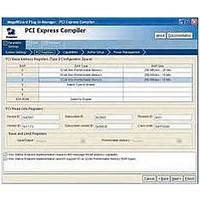
PCI Express Compiler, x8 Link Width
License
Renewal License
Lead Free Status / RoHS Status
na
Lead Free Status / RoHS Status
na


Simple DMA Example Design
5–8
PCI Express Compiler User Guide
32-bit BAR0
32-bit BAR1
64-bit BAR1:0
32-bit BAR2
32-bit BAR3
64-bit BAR3:2
32-bit BAR4
32-bit BAR5
64-bit BAR5:4
Expansion ROM BAR Not implemented by Example Design; behavior is unpredictable.
I/O Space BAR (any)
Table 5–2. Example Design BAR Map
Memory BAR
Maps to 32-KByte target memory block. Lower address bits select the RAM locations to
be read and written. Address bits 15 and above are ignored.
Maps to control register block. For details, see
Registers.
Maps to 32-KByte target memory block. Lower address bits select the RAM locations to
be read and written. Address bits 15 and above are ignored.
Not implemented by Example Design; behavior is unpredictable.
For more information on setting up the DMA channel and registers,
including the base address registers (BARs) for controlling the DMA
channel, see the following section,
Map”.
Example Design BAR/Address Map
The example design maps received memory transactions to either the
target memory block or the control register block based on which BAR the
transaction matched. There are multiple BARs that map to each of these
blocks to maximize interoperability with different variation files.
Table 5–2
The example design control register block is used primarily to set up
DMA channel operations. The control register block sets the addresses,
size, and attributes of the DMA channel operation. Executing a DMA
channel operation includes the following steps:
1.
2.
3.
●
Writing the PCI Express address to the registers at offset 0x00 and
0x04.
Writing the master memory block address to the register at offset
0x14.
Writing the length of the requested operation to the register at offset
0x08.
PCI Express Compiler Version 6.1
Data generator function that can alternatively be the source of
data for memory write transactions initiated by the DMA
channel.
shows the mapping.
Mapping
“Example Design BAR/Address
Table 5–3
Example Design Control
Altera Corporation
December 2006
Related parts for IPR-PCIE/8
Image
Part Number
Description
Manufacturer
Datasheet
Request
R

Part Number:
Description:
IP CORE Renewal Of IP-PCI/MT32
Manufacturer:
Altera
Datasheet:
Part Number:
Description:
IP CORE Renewal Of IP-PCI/MT64
Manufacturer:
Altera
Datasheet:
Part Number:
Description:
IP CORE Renewal Of IP-PCI/T32
Manufacturer:
Altera
Datasheet:
Part Number:
Description:
IP CORE Renewal Of IP-PCI/T64
Manufacturer:
Altera
Datasheet:

Part Number:
Description:
IP CORE Renewal Of IP-PCIE/1
Manufacturer:
Altera
Datasheet:
Part Number:
Description:
IP CORE Renewal Of IP-PCIE/4
Manufacturer:
Altera
Datasheet:
Part Number:
Description:
IP NIOS II MEGACORE RENEW
Manufacturer:
Altera
Datasheet:
Part Number:
Description:
IP CORE Renewal Of IP-XAUIPCS
Manufacturer:
Altera
Datasheet:

Part Number:
Description:
CPLD, EP610 Family, ECMOS Process, 300 Gates, 16 Macro Cells, 16 Reg., 16 User I/Os, 5V Supply, 35 Speed Grade, 24DIP
Manufacturer:
Altera Corporation
Datasheet:
Part Number:
Description:
CPLD, EP610 Family, ECMOS Process, 300 Gates, 16 Macro Cells, 16 Reg., 16 User I/Os, 5V Supply, 15 Speed Grade, 24DIP
Manufacturer:
Altera Corporation
Datasheet:
Part Number:
Description:
Manufacturer:
Altera Corporation
Datasheet: