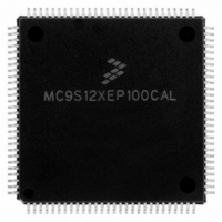
MC9S12XEP100CAL Freescale Semiconductor, MC9S12XEP100CAL Datasheet - Page 211

MC9S12XEP100CAL
Manufacturer Part Number
MC9S12XEP100CAL
Description
IC MCU 16BIT 1M FLASH 112-LQFP
Manufacturer
Freescale Semiconductor
Series
HCS12r
Datasheet
1.MC9S12XEP768CAL.pdf
(1328 pages)
Specifications of MC9S12XEP100CAL
Core Processor
HCS12X
Core Size
16-Bit
Speed
50MHz
Connectivity
CAN, EBI/EMI, I²C, IrDA, SCI, SPI
Peripherals
LVD, POR, PWM, WDT
Number Of I /o
91
Program Memory Size
1MB (1M x 8)
Program Memory Type
FLASH
Eeprom Size
4K x 8
Ram Size
64K x 8
Voltage - Supply (vcc/vdd)
1.72 V ~ 5.5 V
Data Converters
A/D 16x12b
Oscillator Type
External
Operating Temperature
-40°C ~ 85°C
Package / Case
112-LQFP
Processor Series
S12XE
Core
HCS12
Data Bus Width
16 bit
Data Ram Size
64 KB
Interface Type
CAN/SCI/SPI
Maximum Clock Frequency
50 MHz
Number Of Programmable I/os
91
Number Of Timers
25
Maximum Operating Temperature
+ 85 C
Mounting Style
SMD/SMT
3rd Party Development Tools
EWHCS12
Development Tools By Supplier
KIT33812ECUEVME, EVB9S12XEP100, DEMO9S12XEP100
Minimum Operating Temperature
- 40 C
On-chip Adc
16-ch x 12-bit
Package
112LQFP
Family Name
HCS12X
Maximum Speed
50 MHz
Operating Supply Voltage
1.8|2.8|5 V
For Use With
EVB9S12XEP100 - BOARD EVAL FOR MC9S12XEP100DEMO9S12XEP100 - BOARD DEMO FOR MC9S12XEP100
Lead Free Status / RoHS Status
Lead free / RoHS Compliant
Available stocks
Company
Part Number
Manufacturer
Quantity
Price
Company:
Part Number:
MC9S12XEP100CAL
Manufacturer:
TOSHIBA
Quantity:
72
Company:
Part Number:
MC9S12XEP100CAL
Manufacturer:
Freescale Semiconductor
Quantity:
10 000
- Current page: 211 of 1328
- Download datasheet (9Mb)
3.4.2.1.1
Expansion of the CPU Local Address Map
The program page index register in MMC allows accessing up to 4 Mbyte of FLASH or ROM in the global
memory map by using the eight page index bits to page 256 16 Kbyte blocks into the program page
window located from address 0x8000 to address 0xBFFF in the local CPU memory map.
The page value for the program page window is stored in the PPAGE register. The value of the PPAGE
register can be read or written by normal memory accesses as well as by the CALL and RTC instructions
(see
Control registers, vector space and parts of the on-chip memories are located in unpaged portions of the
64-kilobyte local CPU address space.
The starting address of an interrupt service routine must be located in unpaged memory unless the user is
certain that the PPAGE register will be set to the appropriate value when the service routine is called.
However an interrupt service routine can call other routines that are in paged memory. The upper 16-
kilobyte block of the local CPU memory space (0xC000–0xFFFF) is unpaged. It is recommended that all
reset and interrupt vectors point to locations in this area or to the other unpaged sections of the local CPU
memory map.
Table 3-16
PPAGE register value and value of the ROMHM bit in the MMCCTL1 register.
The RAM page index register allows accessing up to 1 Mbyte –2 Kbytes of RAM in the global memory
map by using the eight RPAGE index bits to page 4 Kbyte blocks into the RAM page window located in
the local CPU memory space from address 0x1000 to address 0x1FFF. The EEPROM page index register
EPAGE allows accessing up to 256 Kbytes of EEPROM in the system by using the eight EPAGE index
bits to page 1 Kbyte blocks into the EEPROM page window located in the local CPU memory space from
address 0x0800 to address 0x0BFF.
Freescale Semiconductor
Because of an order from the United States International Trade Commission, BGA-packaged product lines and partnumbers
indicated here currently are not available from Freescale for import or sale in the United States prior to September 2010
Section 3.5.1, “CALL and RTC
summarizes mapping of the address bus in Flash/External space based on the address, the
Expansion of the Local Address Map
1. The internal or the external bus is accessed based on the size of the memory resources
implemented on-chip. Please refer to
0xC000–0xFFFF
0x4000–0x7FFF
0x8000–0xBFFF
CPU Address
Local
MC9S12XE-Family Reference Manual Rev. 1.23
Table 3-16. Global FLASH/ROM Allocated
ROMHM
Instructions).
N/A
N/A
N/A
0
1
Figure 1-23
External
Access
No
Yes
Yes
No
No
(1)
1
for further details.
0x7F_4000 –0x7F_7FFF
0x7F_C000–0x7F_FFFF
Chapter 3 Memory Mapping Control (S12XMMCV4)
0x40_0000–0x7F_FFFF
0x14_4000–0x14_7FFF
Global Address
211
Related parts for MC9S12XEP100CAL
Image
Part Number
Description
Manufacturer
Datasheet
Request
R
Part Number:
Description:
Manufacturer:
Freescale Semiconductor, Inc
Datasheet:
Part Number:
Description:
Manufacturer:
Freescale Semiconductor, Inc
Datasheet:
Part Number:
Description:
Manufacturer:
Freescale Semiconductor, Inc
Datasheet:
Part Number:
Description:
Manufacturer:
Freescale Semiconductor, Inc
Datasheet:
Part Number:
Description:
Manufacturer:
Freescale Semiconductor, Inc
Datasheet:
Part Number:
Description:
Manufacturer:
Freescale Semiconductor, Inc
Datasheet:
Part Number:
Description:
Manufacturer:
Freescale Semiconductor, Inc
Datasheet:
Part Number:
Description:
Manufacturer:
Freescale Semiconductor, Inc
Datasheet:
Part Number:
Description:
Manufacturer:
Freescale Semiconductor, Inc
Datasheet:
Part Number:
Description:
Manufacturer:
Freescale Semiconductor, Inc
Datasheet:
Part Number:
Description:
Manufacturer:
Freescale Semiconductor, Inc
Datasheet:
Part Number:
Description:
Manufacturer:
Freescale Semiconductor, Inc
Datasheet:
Part Number:
Description:
Manufacturer:
Freescale Semiconductor, Inc
Datasheet:
Part Number:
Description:
Manufacturer:
Freescale Semiconductor, Inc
Datasheet:
Part Number:
Description:
Manufacturer:
Freescale Semiconductor, Inc
Datasheet:


