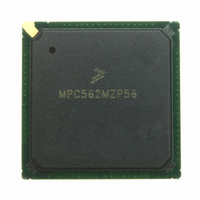
MPC562MZP56 Freescale Semiconductor, MPC562MZP56 Datasheet - Page 760

MPC562MZP56
Manufacturer Part Number
MPC562MZP56
Description
IC MPU 32BIT 56MHZ PPC 388-PBGA
Manufacturer
Freescale Semiconductor
Series
MPC5xxr
Datasheet
1.MPC561MZP56.pdf
(1420 pages)
Specifications of MPC562MZP56
Core Processor
PowerPC
Core Size
32-Bit
Speed
56MHz
Connectivity
CAN, EBI/EMI, SCI, SPI, UART/USART
Peripherals
POR, PWM, WDT
Number Of I /o
64
Program Memory Type
ROMless
Ram Size
32K x 8
Voltage - Supply (vcc/vdd)
2.5 V ~ 2.7 V
Data Converters
A/D 32x10b
Oscillator Type
External
Operating Temperature
-40°C ~ 125°C
Package / Case
388-BGA
Processor Series
MPC5xx
Core
PowerPC
Data Bus Width
32 bit
Data Ram Size
8 KB
Interface Type
SCI, SPI, UART
Maximum Clock Frequency
40 MHz
Number Of Programmable I/os
56
Number Of Timers
22
Operating Supply Voltage
2.6 V to 5 V
Maximum Operating Temperature
+ 85 C
Mounting Style
SMD/SMT
Minimum Operating Temperature
- 40 C
On-chip Adc
2 (10 bit, 32 Channel)
For Use With
MPC564EVB - KIT EVAL FOR MPC561/562/563/564
Lead Free Status / RoHS Status
Request inventory verification / Request inventory verification
Eeprom Size
-
Program Memory Size
-
Lead Free Status / Rohs Status
No
Available stocks
Company
Part Number
Manufacturer
Quantity
Price
Company:
Part Number:
MPC562MZP56
Manufacturer:
FREESCAL
Quantity:
204
Company:
Part Number:
MPC562MZP56
Manufacturer:
Freescale Semiconductor
Quantity:
10 000
Part Number:
MPC562MZP56
Manufacturer:
FREESCALE
Quantity:
20 000
Company:
Part Number:
MPC562MZP56R2
Manufacturer:
RFT
Quantity:
1 441
Company:
Part Number:
MPC562MZP56R2
Manufacturer:
Freescale Semiconductor
Quantity:
10 000
- Current page: 760 of 1420
- Download datasheet (11Mb)
Modular Input/Output Subsystem (MIOS14)
17.9.1.1
The MDASM has one dedicated external signal. This signal is used in input or in output depending on the
selected mode. When in input, it allows the MDASM to perform input capture, input pulse width
measurement and input period measurement. When in output, it allows output compare, single shot output
pulse, single output compare and output port bit operations as well as output pulse width modulation.
17.9.2
The MDASM contains two timing channels A and B associated with the same input/output signal. The
dual action submodule is so called because its timing channel configuration allows two events (input
capture or output compare) to occur before software intervention is required.
Six operating modes allow the software to use the MDASM’s input capture and output compare functions
to perform pulse width measurement, period measurement, single pulse generation and continuous pulse
width generation, as well as standard input capture and output compare. The MDASM can also work as a
single I/O signal. See
Channel A comprises one 16-bit data register and one 16-bit comparator. Channel B also consists of one
16-bit data register and one 16-bit comparator, however, internally, channel B has two data registers B1
and B2, and the operating mode determines which register is accessed by the software:
Register contents are always transferred automatically at the correct time so that the minimum pulse
(measurement or generation) is just one 16-bit counter bus count. The A and B data registers are always
read/write registers, accessible via the MIOB.
In the input modes, the edge detect circuitry triggers a capture whenever a rising or falling edge (as defined
by the EDPOL bit) is applied to the input signal. The signal on the input signal is Schmitt triggered and
synchronized with the MIOS14 CLOCK.
In the disable mode (DIS) and in the input modes, the PIN bit reflects the state present on the input signal
(after being Schmitt triggered and synchronized). In the output modes the PIN bit reflects the value present
on the output flip-flop. The output flip-flop is used in output modes to hold the logic level applied to the
output signal.
17-28
•
•
•
In the input modes (IPWM, IPM and IC), registers A and B2 are used to hold the captured values;
in these modes, the B1 register is used as a temporary latch for channel B.
In the output compare modes (OCB and OCAB), registers A and B2 are used to define the output
pulse; register B1 is not used in these modes.
In the output pulse width modulation mode (OPWM), registers A and B1 are used as primary
registers and hidden register B2 is used as a double buffer for channel B.
MDASM Description
MDASM Signal Functions
In disable mode, the signal becomes a high impedance input and the input
level on this signal is reflected by the state of the PIN bit in the
MDASMSCR register.
Table 17-16
MPC561/MPC563 Reference Manual, Rev. 1.2
for details.
NOTE
Freescale Semiconductor
Related parts for MPC562MZP56
Image
Part Number
Description
Manufacturer
Datasheet
Request
R
Part Number:
Description:
Mpc562 32 Bit Powerpc Microcontroller
Manufacturer:
Freescale Semiconductor, Inc
Datasheet:

Part Number:
Description:
MPC5 1K0 5%
Manufacturer:
TE Connectivity
Datasheet:

Part Number:
Description:
MPC5 500R 5%
Manufacturer:
TE Connectivity
Datasheet:

Part Number:
Description:
MPC5 5K0 5%
Manufacturer:
Tyco Electronics
Datasheet:

Part Number:
Description:
MPC5 5R0 5%
Manufacturer:
Tyco Electronics
Datasheet:

Part Number:
Description:
MPC5 50K 5%
Manufacturer:
Tyco Electronics
Datasheet:
Part Number:
Description:
Manufacturer:
Freescale Semiconductor, Inc
Datasheet:
Part Number:
Description:
Manufacturer:
Freescale Semiconductor, Inc
Datasheet:
Part Number:
Description:
Manufacturer:
Freescale Semiconductor, Inc
Datasheet:
Part Number:
Description:
Manufacturer:
Freescale Semiconductor, Inc
Datasheet:
Part Number:
Description:
Manufacturer:
Freescale Semiconductor, Inc
Datasheet:


