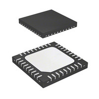
R5F213J6CNNP#U0 Renesas Electronics America, R5F213J6CNNP#U0 Datasheet - Page 180

R5F213J6CNNP#U0
Manufacturer Part Number
R5F213J6CNNP#U0
Description
MCU 1KB FLASH 32K ROM 36-QFN
Manufacturer
Renesas Electronics America
Series
R8C/3x/3JCr
Datasheet
1.R5F213J6CNNPU0.pdf
(750 pages)
Specifications of R5F213J6CNNP#U0
Core Processor
R8C
Core Size
16/32-Bit
Speed
20MHz
Connectivity
I²C, LIN, SIO, SSU, UART/USART
Peripherals
POR, PWM, Voltage Detect, WDT
Number Of I /o
31
Program Memory Size
32KB (32K x 8)
Program Memory Type
FLASH
Ram Size
2.5K x 8
Voltage - Supply (vcc/vdd)
1.8 V ~ 5.5 V
Data Converters
A/D 10x10b, D/A 2x8b
Oscillator Type
Internal
Operating Temperature
-20°C ~ 85°C
Package / Case
36-WQFN Exposed Pad, 36-HWQFN
Lead Free Status / RoHS Status
Lead free / RoHS Compliant
Eeprom Size
-
Available stocks
Company
Part Number
Manufacturer
Quantity
Price
- Current page: 180 of 750
- Download datasheet (8Mb)
R8C/3JC Group
REJ09B0602-0100 Rev.1.00
May 12, 2010
Figure 11.3
11.3.4
Address Bus
CPU Clock
Data Bus
The following describes an interrupt sequence which is performed from when an interrupt request is
acknowledged until the interrupt routine is executed.
When an interrupt request is generated while an instruction is being executed, the CPU determines its interrupt
priority level after the instruction is completed. The CPU starts the interrupt sequence from the following cycle.
However, for the SMOVB, SMOVF, SSTR, or RMPA instruction, if an interrupt request is generated while the
instruction is being executed, the MCU suspends the instruction to start the interrupt sequence. The interrupt
sequence is performed as indicated below.
Figure 11.3 shows the Time Required for Executing Interrupt Sequence.
(1) The CPU obtains interrupt information (interrupt number and interrupt request level) by reading address
(2) The FLG register is saved to a temporary register
(3) The I, D and U flags in the FLG register are set as follows:
(4) The CPU internal temporary register
(5) The PC is saved on the stack.
(6) The interrupt priority level of the acknowledged interrupt is set in the IPL.
(7) The starting address of the interrupt routine set in the interrupt vector is stored in the PC.
After the interrupt sequence is completed, instructions are executed from the starting address of the interrupt
routine.
Notes:
Note:
WR
RD
The indeterminate state depends on the instruction queue buffer.
A read cycle occurs when the instruction queue buffer is ready to acknowledge instructions.
00000h. The IR bit for the corresponding interrupt is set to 0 (no interrupt requested).
sequence.
The I flag is set to 0 (interrupts disabled).
The D flag is set to 0 (single-step interrupt disabled).
The U flag is set to 0 (ISP selected).
However, the U flag does not change state if an INT instruction for software interrupt number 32 to 63 is
executed.
1. These registers cannot be accessed by the user.
2. Refer to 11.7 Timer RC Interrupt, Timer RD Interrupt, Synchronous Serial Communication Unit
Interrupt Sequence
Interrupt, I
Interrupt Request Sources) for the IR bit operations of the timer RC Interrupt, timer RD Interrupt,
Synchronous Serial Communication unit Interrupt, and the I
1
Time Required for Executing Interrupt Sequence
2
Address
0000h
information
Interrupt
3
2
C bus Interface Interrupt, and Flash Memory Interrupt (Interrupts with Multiple
4
5
Undefined
Undefined
Undefined
6
7
(1)
is saved on the stack.
8
SP-2 SP-1
9
contents
SP-2
10
(1)
contents
SP-1
in the CPU immediately before entering the interrupt
SP-4
11
contents
SP-4
12
SP-3
contents
SP-3
2
13
C bus Interface Interrupt.
VEC
14
contents
VEC
15
VEC+1
contents
VEC+1
16
17
(2)
VEC+2
contents
VEC+2
18
Page 149 of 715
11. Interrupts
19
PC
20
Related parts for R5F213J6CNNP#U0
Image
Part Number
Description
Manufacturer
Datasheet
Request
R

Part Number:
Description:
KIT STARTER FOR M16C/29
Manufacturer:
Renesas Electronics America
Datasheet:

Part Number:
Description:
KIT STARTER FOR R8C/2D
Manufacturer:
Renesas Electronics America
Datasheet:

Part Number:
Description:
R0K33062P STARTER KIT
Manufacturer:
Renesas Electronics America
Datasheet:

Part Number:
Description:
KIT STARTER FOR R8C/23 E8A
Manufacturer:
Renesas Electronics America
Datasheet:

Part Number:
Description:
KIT STARTER FOR R8C/25
Manufacturer:
Renesas Electronics America
Datasheet:

Part Number:
Description:
KIT STARTER H8S2456 SHARPE DSPLY
Manufacturer:
Renesas Electronics America
Datasheet:

Part Number:
Description:
KIT STARTER FOR R8C38C
Manufacturer:
Renesas Electronics America
Datasheet:

Part Number:
Description:
KIT STARTER FOR R8C35C
Manufacturer:
Renesas Electronics America
Datasheet:

Part Number:
Description:
KIT STARTER FOR R8CL3AC+LCD APPS
Manufacturer:
Renesas Electronics America
Datasheet:

Part Number:
Description:
KIT STARTER FOR RX610
Manufacturer:
Renesas Electronics America
Datasheet:

Part Number:
Description:
KIT STARTER FOR R32C/118
Manufacturer:
Renesas Electronics America
Datasheet:

Part Number:
Description:
KIT DEV RSK-R8C/26-29
Manufacturer:
Renesas Electronics America
Datasheet:

Part Number:
Description:
KIT STARTER FOR SH7124
Manufacturer:
Renesas Electronics America
Datasheet:

Part Number:
Description:
KIT STARTER FOR H8SX/1622
Manufacturer:
Renesas Electronics America
Datasheet:

Part Number:
Description:
KIT DEV FOR SH7203
Manufacturer:
Renesas Electronics America
Datasheet:


