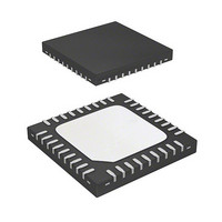
R5F213J6CNNP#U0 Renesas Electronics America, R5F213J6CNNP#U0 Datasheet - Page 247

R5F213J6CNNP#U0
Manufacturer Part Number
R5F213J6CNNP#U0
Description
MCU 1KB FLASH 32K ROM 36-QFN
Manufacturer
Renesas Electronics America
Series
R8C/3x/3JCr
Datasheet
1.R5F213J6CNNPU0.pdf
(750 pages)
Specifications of R5F213J6CNNP#U0
Core Processor
R8C
Core Size
16/32-Bit
Speed
20MHz
Connectivity
I²C, LIN, SIO, SSU, UART/USART
Peripherals
POR, PWM, Voltage Detect, WDT
Number Of I /o
31
Program Memory Size
32KB (32K x 8)
Program Memory Type
FLASH
Ram Size
2.5K x 8
Voltage - Supply (vcc/vdd)
1.8 V ~ 5.5 V
Data Converters
A/D 10x10b, D/A 2x8b
Oscillator Type
Internal
Operating Temperature
-20°C ~ 85°C
Package / Case
36-WQFN Exposed Pad, 36-HWQFN
Lead Free Status / RoHS Status
Lead free / RoHS Compliant
Eeprom Size
-
Available stocks
Company
Part Number
Manufacturer
Quantity
Price
- Current page: 247 of 750
- Download datasheet (8Mb)
R8C/3JC Group
REJ09B0602-0100 Rev.1.00
May 12, 2010
17.5
Table 17.4
Note:
Count source
Count operations
Divide ratio
Count start condition
Count stop conditions • 0 (count stops) is written to the TSTART bit in the TRACR register.
Interrupt request
generation timing
TRAIO pin function
TRAO pin function
Read from timer
Write to timer
Selectable functions
In event counter mode, external signal inputs to the TRAIO pin are counted (refer to Table 17.4 Event Counter
Mode Specifications).
1. The level of the output pulse becomes the level when the pulse output starts when the TRAMR
register is written to.
Event Counter Mode
Item
Event Counter Mode Specifications
External signal which is input to TRAIO pin (active edge selectable by a program)
• Decrement
• When the timer underflows, the contents of the reload register are reloaded and
1/(n+1)(m+1)
n: setting value of TRAPRE register, m: setting value of TRA register
1 (count starts) is written to the TSTART bit in the TRACR register.
• 1 (count forcibly stops) is written to the TSTOP bit in the TRACR register.
When timer RA underflows [timer RA interrupt].
Count source input
Programmable I/O port or pulse output
The count value can be read by reading registers TRA and TRAPRE.
• When registers TRAPRE and TRA are written while the count is stopped, values
• When registers TRAPRE and TRA are written during the count, values are
• TRAIO input polarity switch function
• Count source input pin select function
• Pulse output function
• Digital filter function
• Event input control function
the count is continued.
are written to both the reload register and counter.
written to the reload register and counter (refer to 17.3.2 Timer Write Control
during Count Operation ).
The active edge of the count source is selected by the TEDGSEL bit in the
TRAIOC register.
P1_5 or P1_7 is selected by bits TRAIOSEL0 to TRAIOSEL1 in the TRASR
register.
Pulses of inverted polarity can be output from the TRAO pin each time the timer
underflows (selectable by the TOENA bit in the TRAIOC register).
Whether enabling or disabling the digital filter and the sampling frequency is
selected by bits TIPF0 and TIPF1 in the TRAIOC register.
The enabled period for the event input to the TRAIO pin is selected by bits
TIOGT0 and TIOGT1 in the TRAIOC register.
Specification
(1)
(1)
Page 216 of 715
17. Timer RA
Related parts for R5F213J6CNNP#U0
Image
Part Number
Description
Manufacturer
Datasheet
Request
R

Part Number:
Description:
KIT STARTER FOR M16C/29
Manufacturer:
Renesas Electronics America
Datasheet:

Part Number:
Description:
KIT STARTER FOR R8C/2D
Manufacturer:
Renesas Electronics America
Datasheet:

Part Number:
Description:
R0K33062P STARTER KIT
Manufacturer:
Renesas Electronics America
Datasheet:

Part Number:
Description:
KIT STARTER FOR R8C/23 E8A
Manufacturer:
Renesas Electronics America
Datasheet:

Part Number:
Description:
KIT STARTER FOR R8C/25
Manufacturer:
Renesas Electronics America
Datasheet:

Part Number:
Description:
KIT STARTER H8S2456 SHARPE DSPLY
Manufacturer:
Renesas Electronics America
Datasheet:

Part Number:
Description:
KIT STARTER FOR R8C38C
Manufacturer:
Renesas Electronics America
Datasheet:

Part Number:
Description:
KIT STARTER FOR R8C35C
Manufacturer:
Renesas Electronics America
Datasheet:

Part Number:
Description:
KIT STARTER FOR R8CL3AC+LCD APPS
Manufacturer:
Renesas Electronics America
Datasheet:

Part Number:
Description:
KIT STARTER FOR RX610
Manufacturer:
Renesas Electronics America
Datasheet:

Part Number:
Description:
KIT STARTER FOR R32C/118
Manufacturer:
Renesas Electronics America
Datasheet:

Part Number:
Description:
KIT DEV RSK-R8C/26-29
Manufacturer:
Renesas Electronics America
Datasheet:

Part Number:
Description:
KIT STARTER FOR SH7124
Manufacturer:
Renesas Electronics America
Datasheet:

Part Number:
Description:
KIT STARTER FOR H8SX/1622
Manufacturer:
Renesas Electronics America
Datasheet:

Part Number:
Description:
KIT DEV FOR SH7203
Manufacturer:
Renesas Electronics America
Datasheet:


