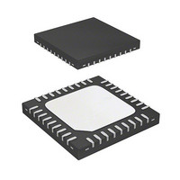
R5F213J6CNNP#U0 Renesas Electronics America, R5F213J6CNNP#U0 Datasheet - Page 738

R5F213J6CNNP#U0
Manufacturer Part Number
R5F213J6CNNP#U0
Description
MCU 1KB FLASH 32K ROM 36-QFN
Manufacturer
Renesas Electronics America
Series
R8C/3x/3JCr
Datasheet
1.R5F213J6CNNPU0.pdf
(750 pages)
Specifications of R5F213J6CNNP#U0
Core Processor
R8C
Core Size
16/32-Bit
Speed
20MHz
Connectivity
I²C, LIN, SIO, SSU, UART/USART
Peripherals
POR, PWM, Voltage Detect, WDT
Number Of I /o
31
Program Memory Size
32KB (32K x 8)
Program Memory Type
FLASH
Ram Size
2.5K x 8
Voltage - Supply (vcc/vdd)
1.8 V ~ 5.5 V
Data Converters
A/D 10x10b, D/A 2x8b
Oscillator Type
Internal
Operating Temperature
-20°C ~ 85°C
Package / Case
36-WQFN Exposed Pad, 36-HWQFN
Lead Free Status / RoHS Status
Lead free / RoHS Compliant
Eeprom Size
-
Available stocks
Company
Part Number
Manufacturer
Quantity
Price
- Current page: 738 of 750
- Download datasheet (8Mb)
R8C/3JC Group
REJ09B0602-0100 Rev.1.00
May 12, 2010
34.18 Notes on Noise
34.19 Note on Supply Voltage Fluctuation
Figure 34.7
34.18.1 Inserting a Bypass Capacitor between VCC and VSS Pins as a Countermeasure
34.18.2 Countermeasures against Noise Error of Port Control Registers
After reset is deasserted, the supply voltage applied to the VCC pin must meet either or both the allowable ripple
voltage Vr (vcc) or ripple voltage falling gradient dVr (vcc)/dt shown in Figure 34.7.
VCC
Connect a bypass capacitor (approximately 0.1 µ F) using the shortest and thickest wire possible.
During rigorous noise testing or the like, external noise (mainly power supply system noise) can exceed the
capacity of the MCU’s internal noise control circuitry. In such cases the contents of the port related registers
may be changed.
As a firmware countermeasure, it is recommended that the port registers, port direction registers, and pull-up
control registers be reset periodically. However, examine the control processing fully before introducing the
reset routine as conflicts may be created between the reset routine and interrupt routines.
Vr (vcc)
dVr (vcc)/dt
Symbol
against Noise and Latch-up
Definition of ripple voltage
Allowable ripple voltage
Ripple voltage falling gradient
Parameter
Min.
Standard
Typ.
0.1 VCC
Max.
10
34. Usage Notes
Page 707 of 715
V/ms
Unit
V
Vr (vcc)
Related parts for R5F213J6CNNP#U0
Image
Part Number
Description
Manufacturer
Datasheet
Request
R

Part Number:
Description:
KIT STARTER FOR M16C/29
Manufacturer:
Renesas Electronics America
Datasheet:

Part Number:
Description:
KIT STARTER FOR R8C/2D
Manufacturer:
Renesas Electronics America
Datasheet:

Part Number:
Description:
R0K33062P STARTER KIT
Manufacturer:
Renesas Electronics America
Datasheet:

Part Number:
Description:
KIT STARTER FOR R8C/23 E8A
Manufacturer:
Renesas Electronics America
Datasheet:

Part Number:
Description:
KIT STARTER FOR R8C/25
Manufacturer:
Renesas Electronics America
Datasheet:

Part Number:
Description:
KIT STARTER H8S2456 SHARPE DSPLY
Manufacturer:
Renesas Electronics America
Datasheet:

Part Number:
Description:
KIT STARTER FOR R8C38C
Manufacturer:
Renesas Electronics America
Datasheet:

Part Number:
Description:
KIT STARTER FOR R8C35C
Manufacturer:
Renesas Electronics America
Datasheet:

Part Number:
Description:
KIT STARTER FOR R8CL3AC+LCD APPS
Manufacturer:
Renesas Electronics America
Datasheet:

Part Number:
Description:
KIT STARTER FOR RX610
Manufacturer:
Renesas Electronics America
Datasheet:

Part Number:
Description:
KIT STARTER FOR R32C/118
Manufacturer:
Renesas Electronics America
Datasheet:

Part Number:
Description:
KIT DEV RSK-R8C/26-29
Manufacturer:
Renesas Electronics America
Datasheet:

Part Number:
Description:
KIT STARTER FOR SH7124
Manufacturer:
Renesas Electronics America
Datasheet:

Part Number:
Description:
KIT STARTER FOR H8SX/1622
Manufacturer:
Renesas Electronics America
Datasheet:

Part Number:
Description:
KIT DEV FOR SH7203
Manufacturer:
Renesas Electronics America
Datasheet:


