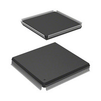
HD6417727F100CV Renesas Electronics America, HD6417727F100CV Datasheet - Page 156

HD6417727F100CV
Manufacturer Part Number
HD6417727F100CV
Description
SH3-DSP, LEAD FREE
Manufacturer
Renesas Electronics America
Series
SuperH® SH7700r
Datasheet
1.HD6417727BP100CV.pdf
(1098 pages)
Specifications of HD6417727F100CV
Core Processor
SH-3 DSP
Core Size
32-Bit
Speed
100MHz
Connectivity
FIFO, SCI, SIO, SmartCard, USB
Peripherals
DMA, LCD, POR, WDT
Number Of I /o
104
Program Memory Type
ROMless
Ram Size
32K x 8
Voltage - Supply (vcc/vdd)
1.6 V ~ 2.05 V
Data Converters
A/D 6x10b; D/A 2x8b
Oscillator Type
Internal
Operating Temperature
-20°C ~ 75°C
Package / Case
240-QFP Exposed Pad, 240-eQFP, 240-HQFP
Cpu Family
SuperH
Device Core Size
32b
Frequency (max)
100MHz
Interface Type
SCI/USB
Program Memory Size
Not Required
Total Internal Ram Size
16KB
# I/os (max)
104
Number Of Timers - General Purpose
4
Operating Supply Voltage (typ)
1.8/3.3V
Operating Supply Voltage (max)
2.05/3.6V
Operating Supply Voltage (min)
1.6/2.6V
On-chip Adc
6-chx10-bit
On-chip Dac
2-chx8-bit
Instruction Set Architecture
RISC
Operating Temp Range
-20C to 75C
Operating Temperature Classification
Commercial
Mounting
Surface Mount
Pin Count
240
Package Type
HQFP
Lead Free Status / RoHS Status
Lead free / RoHS Compliant
Eeprom Size
-
Program Memory Size
-
Lead Free Status / Rohs Status
Compliant
- Current page: 156 of 1098
- Download datasheet (7Mb)
Section 3 Memory Management Unit (MMU)
When address translation from virtual memory to physical memory is performed using the MMU,
it may occur that the relevant translation information is not recorded in the MMU, with the result
that one process may inadvertently access the virtual memory allocated to another process. In this
case, the MMU will generate an exception, change the physical memory mapping, and record the
new address translation information.
Although the functions of the MMU could also be implemented by software alone, the need for
translation to be performed by software each time a process accesses physical memory would
result in poor efficiency. For this reason, a buffer for address translation (translation look-aside
buffer: TLB) is provided in hardware to hold frequently used address translation information. The
TLB can be described as a cache for storing address translation information. Unlike cache
memory, however, if address translation fails, that is, if an exception is generated, switching of
address translation information is normally performed by software. This makes it possible for
memory management to be performed flexibly by software.
The MMU has two methods of mapping from virtual memory to physical memory: a paging
method using fixed-length address translation, and a segment method using variable-length
address translation. With the paging method, the unit of translation is a fixed-size address space
(usually of 1 to 64 kbytes) called a page.
In the following text, the SH7727 address space in virtual memory is referred to as logical address
space, and address space in physical memory as physical memory space.
Rev.6.00 Mar. 27, 2009 Page 98 of 1036
REJ09B0254-0600
Related parts for HD6417727F100CV
Image
Part Number
Description
Manufacturer
Datasheet
Request
R

Part Number:
Description:
KIT STARTER FOR M16C/29
Manufacturer:
Renesas Electronics America
Datasheet:

Part Number:
Description:
KIT STARTER FOR R8C/2D
Manufacturer:
Renesas Electronics America
Datasheet:

Part Number:
Description:
R0K33062P STARTER KIT
Manufacturer:
Renesas Electronics America
Datasheet:

Part Number:
Description:
KIT STARTER FOR R8C/23 E8A
Manufacturer:
Renesas Electronics America
Datasheet:

Part Number:
Description:
KIT STARTER FOR R8C/25
Manufacturer:
Renesas Electronics America
Datasheet:

Part Number:
Description:
KIT STARTER H8S2456 SHARPE DSPLY
Manufacturer:
Renesas Electronics America
Datasheet:

Part Number:
Description:
KIT STARTER FOR R8C38C
Manufacturer:
Renesas Electronics America
Datasheet:

Part Number:
Description:
KIT STARTER FOR R8C35C
Manufacturer:
Renesas Electronics America
Datasheet:

Part Number:
Description:
KIT STARTER FOR R8CL3AC+LCD APPS
Manufacturer:
Renesas Electronics America
Datasheet:

Part Number:
Description:
KIT STARTER FOR RX610
Manufacturer:
Renesas Electronics America
Datasheet:

Part Number:
Description:
KIT STARTER FOR R32C/118
Manufacturer:
Renesas Electronics America
Datasheet:

Part Number:
Description:
KIT DEV RSK-R8C/26-29
Manufacturer:
Renesas Electronics America
Datasheet:

Part Number:
Description:
KIT STARTER FOR SH7124
Manufacturer:
Renesas Electronics America
Datasheet:

Part Number:
Description:
KIT STARTER FOR H8SX/1622
Manufacturer:
Renesas Electronics America
Datasheet:

Part Number:
Description:
KIT DEV FOR SH7203
Manufacturer:
Renesas Electronics America
Datasheet:


