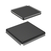
HD6417727F100CV Renesas Electronics America, HD6417727F100CV Datasheet - Page 973

HD6417727F100CV
Manufacturer Part Number
HD6417727F100CV
Description
SH3-DSP, LEAD FREE
Manufacturer
Renesas Electronics America
Series
SuperH® SH7700r
Datasheet
1.HD6417727BP100CV.pdf
(1098 pages)
Specifications of HD6417727F100CV
Core Processor
SH-3 DSP
Core Size
32-Bit
Speed
100MHz
Connectivity
FIFO, SCI, SIO, SmartCard, USB
Peripherals
DMA, LCD, POR, WDT
Number Of I /o
104
Program Memory Type
ROMless
Ram Size
32K x 8
Voltage - Supply (vcc/vdd)
1.6 V ~ 2.05 V
Data Converters
A/D 6x10b; D/A 2x8b
Oscillator Type
Internal
Operating Temperature
-20°C ~ 75°C
Package / Case
240-QFP Exposed Pad, 240-eQFP, 240-HQFP
Cpu Family
SuperH
Device Core Size
32b
Frequency (max)
100MHz
Interface Type
SCI/USB
Program Memory Size
Not Required
Total Internal Ram Size
16KB
# I/os (max)
104
Number Of Timers - General Purpose
4
Operating Supply Voltage (typ)
1.8/3.3V
Operating Supply Voltage (max)
2.05/3.6V
Operating Supply Voltage (min)
1.6/2.6V
On-chip Adc
6-chx10-bit
On-chip Dac
2-chx8-bit
Instruction Set Architecture
RISC
Operating Temp Range
-20C to 75C
Operating Temperature Classification
Commercial
Mounting
Surface Mount
Pin Count
240
Package Type
HQFP
Lead Free Status / RoHS Status
Lead free / RoHS Compliant
Eeprom Size
-
Program Memory Size
-
Lead Free Status / Rohs Status
Compliant
- Current page: 973 of 1098
- Download datasheet (7Mb)
31.1
The SH7727 incorporates a user-debugging interface (H-UDI) and advanced user debugger
(AUD) for program debugging.
31.2
The H-UDI (user-debugging interface) performs on-chip debugging which is supported by the
SH7727. The H-UDI described here is a serial interface which is compatible with JTAG (Joint
Test Action Group, IEEE Standard 1149.1 and IEEE Standard Test Access Port and Boundary-
Scan Architecture) specifications.
The H-UDI in the SH7727 supports a boundary scan mode, and is also used for emulator
connection.
When using an emulator, H-UDI functions should not be used. Refer to the emulator manual for
the method of connecting the emulator.
31.2.1
TCK: H-UDI serial data input/output clock pin. Data is serially supplied to the H-UDI from the
data input pin (TDI), and output from the data output pin (TDO), in synchronization with this
clock.
TMS: Mode select input pin. The state of the TAP control circuit is determined by changing this
signal in synchronization with TCK. The protocol conforms to the JTAG standard (IEEE Std.
1149.1).
TRST: H-UDI reset input pin. Input is accepted asynchronously with respect to TCK, and when
low, the H-UDI is reset. See section 31.4.2, Reset Configuration, for more information.
TDI: H-UDI serial data input pin. Data transfer to the H-UDI is executed by changing this signal
in synchronization with TCK.
TDO: H-UDI serial data output pin. Data output from the H-UDI is executed by reading this
signal in synchronization with TCK.
ASEMD0: The ASE mode select pin. If a low level is input to the ASEMD0 pin while the
RESETP pin is asserted, ASE mode is entered, and if a high level is input, normal mode is
entered. When using the user system alone and not using an emulator or the H-UDI, a high level
Overview
User Debugging Interface (H-UDI)
Pin Description
Section 31 User-Debugging Interface (H-UDI)
Section 31 User-Debugging Interface (H-UDI)
Rev.6.00 Mar. 27, 2009 Page 915 of 1036
REJ09B0254-0600
Related parts for HD6417727F100CV
Image
Part Number
Description
Manufacturer
Datasheet
Request
R

Part Number:
Description:
KIT STARTER FOR M16C/29
Manufacturer:
Renesas Electronics America
Datasheet:

Part Number:
Description:
KIT STARTER FOR R8C/2D
Manufacturer:
Renesas Electronics America
Datasheet:

Part Number:
Description:
R0K33062P STARTER KIT
Manufacturer:
Renesas Electronics America
Datasheet:

Part Number:
Description:
KIT STARTER FOR R8C/23 E8A
Manufacturer:
Renesas Electronics America
Datasheet:

Part Number:
Description:
KIT STARTER FOR R8C/25
Manufacturer:
Renesas Electronics America
Datasheet:

Part Number:
Description:
KIT STARTER H8S2456 SHARPE DSPLY
Manufacturer:
Renesas Electronics America
Datasheet:

Part Number:
Description:
KIT STARTER FOR R8C38C
Manufacturer:
Renesas Electronics America
Datasheet:

Part Number:
Description:
KIT STARTER FOR R8C35C
Manufacturer:
Renesas Electronics America
Datasheet:

Part Number:
Description:
KIT STARTER FOR R8CL3AC+LCD APPS
Manufacturer:
Renesas Electronics America
Datasheet:

Part Number:
Description:
KIT STARTER FOR RX610
Manufacturer:
Renesas Electronics America
Datasheet:

Part Number:
Description:
KIT STARTER FOR R32C/118
Manufacturer:
Renesas Electronics America
Datasheet:

Part Number:
Description:
KIT DEV RSK-R8C/26-29
Manufacturer:
Renesas Electronics America
Datasheet:

Part Number:
Description:
KIT STARTER FOR SH7124
Manufacturer:
Renesas Electronics America
Datasheet:

Part Number:
Description:
KIT STARTER FOR H8SX/1622
Manufacturer:
Renesas Electronics America
Datasheet:

Part Number:
Description:
KIT DEV FOR SH7203
Manufacturer:
Renesas Electronics America
Datasheet:


