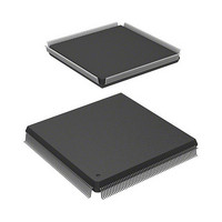
HD6417727F100CV Renesas Electronics America, HD6417727F100CV Datasheet - Page 659

HD6417727F100CV
Manufacturer Part Number
HD6417727F100CV
Description
SH3-DSP, LEAD FREE
Manufacturer
Renesas Electronics America
Series
SuperH® SH7700r
Datasheet
1.HD6417727BP100CV.pdf
(1098 pages)
Specifications of HD6417727F100CV
Core Processor
SH-3 DSP
Core Size
32-Bit
Speed
100MHz
Connectivity
FIFO, SCI, SIO, SmartCard, USB
Peripherals
DMA, LCD, POR, WDT
Number Of I /o
104
Program Memory Type
ROMless
Ram Size
32K x 8
Voltage - Supply (vcc/vdd)
1.6 V ~ 2.05 V
Data Converters
A/D 6x10b; D/A 2x8b
Oscillator Type
Internal
Operating Temperature
-20°C ~ 75°C
Package / Case
240-QFP Exposed Pad, 240-eQFP, 240-HQFP
Cpu Family
SuperH
Device Core Size
32b
Frequency (max)
100MHz
Interface Type
SCI/USB
Program Memory Size
Not Required
Total Internal Ram Size
16KB
# I/os (max)
104
Number Of Timers - General Purpose
4
Operating Supply Voltage (typ)
1.8/3.3V
Operating Supply Voltage (max)
2.05/3.6V
Operating Supply Voltage (min)
1.6/2.6V
On-chip Adc
6-chx10-bit
On-chip Dac
2-chx8-bit
Instruction Set Architecture
RISC
Operating Temp Range
-20C to 75C
Operating Temperature Classification
Commercial
Mounting
Surface Mount
Pin Count
240
Package Type
HQFP
Lead Free Status / RoHS Status
Lead free / RoHS Compliant
Eeprom Size
-
Program Memory Size
-
Lead Free Status / Rohs Status
Compliant
- Current page: 659 of 1098
- Download datasheet (7Mb)
19.5
Note the following when using the SCIF.
1. SCFTDR2 Writing and the TDFE Flag: The TDFE flag in the serial status register 2 (SCSSR2)
2. SCFRDR2 Reading and the RDF Flag: The RDF flag in the serial status register 2 (SCSSR2)
3. Break Detection and Processing: Break signals can be detected by reading the RxD2 pin
4. Sending a Break Signal: The I/O condition and level of the TxD2 pin are determined by the
is set when the number of transmit data bytes written in the transmit FIFO data register 2
(SCFTDR2) has fallen below the transmit trigger number set by bits TTRG1 and TTRG0 in
the FIFO control register 2 (SCFCR2). After TDFE is set, transmit data up to the number of
empty bytes in SCFTDR2 can be written, allowing efficient continuous transmission.
However, if the number of data bytes written in SCFTDR2 is less than or equal to the transmit
trigger number, the TDFE flag will be set to 1 again after being cleared to 0. The TDFE flag
should therefore be cleared to 0 after a number of data bytes exceeding the transmit trigger
number has been written to SCFTDR2.
The number of transmit data bytes in SCFTDR2 can be found from the upper 8 bits of the
FIFO data count set register 2 (SCFDR2).
is set when the number of receive data bytes in the receive FIFO data register 2 (SCFRDR2)
has become equal to or greater than the receive trigger number set by bits RTRG1 and RTRG0
in the FIFO control register 2 (SCFCR2). After RDF is set, receive data equivalent to the
trigger number can be read from SCFRDR2, allowing efficient continuous reception.
However, if the number of data bytes in SCFRDR2 exceeds the trigger number, the RDF flag
will be set to 1 again after being cleared to 0. The RDF flag should therefore be cleared to 0
when 1 has been written to RDF after all receive data has been read.
The number of receive data bytes in SCFRDR2 can be found from the lower 8 bits of the FIFO
data count set register 2 (SCFDR2).
directly when a framing error (FER) is detected. In the break state the input from the RxD2
pin consists of all 0s, so the FER flag is set and the parity error flag (PER) may also be set.
Note that, although transfer of receive data to SCFRDR2 is halted in the break state, the SCIF
receiver continues to operate, so if the BRK flag is cleared to 0 it will be set to 1 again.
SCP4DT bit in the port SC data register 2 (SCPDR2) and bits SCP4MD0 and SCP4MD1 in the
port SC control register 2 (SCPCR2). This feature can be used to send a break signal.
To send a break signal during serial transmission, clear the CP4DT bit to 0 (designating low
level), then set the SCP4MD0 and SCP4MD1 bits to 1 and 0, respectively, and finally clear the
TE bit to 0 (halting transmission). When the TE bit is cleared to 0, the transmitter is initialized
regardless of the current transmission state, and 0 is output from the TxD2 pin.
Usage Notes
Section 19 Serial Communication Interface with FIFO (SCIF)
Rev.6.00 Mar. 27, 2009 Page 601 of 1036
REJ09B0254-0600
Related parts for HD6417727F100CV
Image
Part Number
Description
Manufacturer
Datasheet
Request
R

Part Number:
Description:
KIT STARTER FOR M16C/29
Manufacturer:
Renesas Electronics America
Datasheet:

Part Number:
Description:
KIT STARTER FOR R8C/2D
Manufacturer:
Renesas Electronics America
Datasheet:

Part Number:
Description:
R0K33062P STARTER KIT
Manufacturer:
Renesas Electronics America
Datasheet:

Part Number:
Description:
KIT STARTER FOR R8C/23 E8A
Manufacturer:
Renesas Electronics America
Datasheet:

Part Number:
Description:
KIT STARTER FOR R8C/25
Manufacturer:
Renesas Electronics America
Datasheet:

Part Number:
Description:
KIT STARTER H8S2456 SHARPE DSPLY
Manufacturer:
Renesas Electronics America
Datasheet:

Part Number:
Description:
KIT STARTER FOR R8C38C
Manufacturer:
Renesas Electronics America
Datasheet:

Part Number:
Description:
KIT STARTER FOR R8C35C
Manufacturer:
Renesas Electronics America
Datasheet:

Part Number:
Description:
KIT STARTER FOR R8CL3AC+LCD APPS
Manufacturer:
Renesas Electronics America
Datasheet:

Part Number:
Description:
KIT STARTER FOR RX610
Manufacturer:
Renesas Electronics America
Datasheet:

Part Number:
Description:
KIT STARTER FOR R32C/118
Manufacturer:
Renesas Electronics America
Datasheet:

Part Number:
Description:
KIT DEV RSK-R8C/26-29
Manufacturer:
Renesas Electronics America
Datasheet:

Part Number:
Description:
KIT STARTER FOR SH7124
Manufacturer:
Renesas Electronics America
Datasheet:

Part Number:
Description:
KIT STARTER FOR H8SX/1622
Manufacturer:
Renesas Electronics America
Datasheet:

Part Number:
Description:
KIT DEV FOR SH7203
Manufacturer:
Renesas Electronics America
Datasheet:


