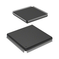
HD6417727F100CV Renesas Electronics America, HD6417727F100CV Datasheet - Page 84

HD6417727F100CV
Manufacturer Part Number
HD6417727F100CV
Description
SH3-DSP, LEAD FREE
Manufacturer
Renesas Electronics America
Series
SuperH® SH7700r
Datasheet
1.HD6417727BP100CV.pdf
(1098 pages)
Specifications of HD6417727F100CV
Core Processor
SH-3 DSP
Core Size
32-Bit
Speed
100MHz
Connectivity
FIFO, SCI, SIO, SmartCard, USB
Peripherals
DMA, LCD, POR, WDT
Number Of I /o
104
Program Memory Type
ROMless
Ram Size
32K x 8
Voltage - Supply (vcc/vdd)
1.6 V ~ 2.05 V
Data Converters
A/D 6x10b; D/A 2x8b
Oscillator Type
Internal
Operating Temperature
-20°C ~ 75°C
Package / Case
240-QFP Exposed Pad, 240-eQFP, 240-HQFP
Cpu Family
SuperH
Device Core Size
32b
Frequency (max)
100MHz
Interface Type
SCI/USB
Program Memory Size
Not Required
Total Internal Ram Size
16KB
# I/os (max)
104
Number Of Timers - General Purpose
4
Operating Supply Voltage (typ)
1.8/3.3V
Operating Supply Voltage (max)
2.05/3.6V
Operating Supply Voltage (min)
1.6/2.6V
On-chip Adc
6-chx10-bit
On-chip Dac
2-chx8-bit
Instruction Set Architecture
RISC
Operating Temp Range
-20C to 75C
Operating Temperature Classification
Commercial
Mounting
Surface Mount
Pin Count
240
Package Type
HQFP
Lead Free Status / RoHS Status
Lead free / RoHS Compliant
Eeprom Size
-
Program Memory Size
-
Lead Free Status / Rohs Status
Compliant
- Current page: 84 of 1098
- Download datasheet (7Mb)
Section 2 CPU
On the other hand, R2 to R9 registers are also used for the DSP data address calculations, see
figure 2.4, when DSP extension is enabled. Another symbol that represents the purpose of the
registers in DSP type instruction is [ ].
DSP type instructions can access X and Y data memory simultaneously. To specify addresses for
X and Y data memory, two address pointer sets are prepared. These are:
R8[Ix], R4, R5[Ax] for X memory access, and R9[Iy], R6, R7[Ay] for Y memory access.
The names (symbol) R2 to R9 are used in the Assembler, but users can use other register names
that represent the purpose of the register in the DSP instruction explicitly. In the assembly
program, user can use an alias for the register. The coding in assembler is as follows.
Rev.6.00 Mar. 27, 2009 Page 26 of 1036
REJ09B0254-0600
Ix: .REG (R8)
31
R0
R1
R2 [As]
R3 [As]
R4 [As, Ax]
R5 [As, Ax]
R6 [Ay]
R7 [Ay]
R8 [Ix, Is]
R9 [Iy]
R10
R11
R12
R13
R14
R15
Figure 2.4 General Purpose Register (DSP Mode)
0
General Registers (DSP mode enabled)
X or Y data transfer operation
Single data transfer operation
R4, R5 [Ax]:
R8 [x]:
R6, R7 [Ay]:
R9 [Iy]:
R2 to R5 [As]: Address register set for memory.
R8 [Is]:
Address register set for X data memory.
Index register for address register set Ax.
Address register set for Y data memory.
Index register for address register set Ay.
Index register for address register set As.
Related parts for HD6417727F100CV
Image
Part Number
Description
Manufacturer
Datasheet
Request
R

Part Number:
Description:
KIT STARTER FOR M16C/29
Manufacturer:
Renesas Electronics America
Datasheet:

Part Number:
Description:
KIT STARTER FOR R8C/2D
Manufacturer:
Renesas Electronics America
Datasheet:

Part Number:
Description:
R0K33062P STARTER KIT
Manufacturer:
Renesas Electronics America
Datasheet:

Part Number:
Description:
KIT STARTER FOR R8C/23 E8A
Manufacturer:
Renesas Electronics America
Datasheet:

Part Number:
Description:
KIT STARTER FOR R8C/25
Manufacturer:
Renesas Electronics America
Datasheet:

Part Number:
Description:
KIT STARTER H8S2456 SHARPE DSPLY
Manufacturer:
Renesas Electronics America
Datasheet:

Part Number:
Description:
KIT STARTER FOR R8C38C
Manufacturer:
Renesas Electronics America
Datasheet:

Part Number:
Description:
KIT STARTER FOR R8C35C
Manufacturer:
Renesas Electronics America
Datasheet:

Part Number:
Description:
KIT STARTER FOR R8CL3AC+LCD APPS
Manufacturer:
Renesas Electronics America
Datasheet:

Part Number:
Description:
KIT STARTER FOR RX610
Manufacturer:
Renesas Electronics America
Datasheet:

Part Number:
Description:
KIT STARTER FOR R32C/118
Manufacturer:
Renesas Electronics America
Datasheet:

Part Number:
Description:
KIT DEV RSK-R8C/26-29
Manufacturer:
Renesas Electronics America
Datasheet:

Part Number:
Description:
KIT STARTER FOR SH7124
Manufacturer:
Renesas Electronics America
Datasheet:

Part Number:
Description:
KIT STARTER FOR H8SX/1622
Manufacturer:
Renesas Electronics America
Datasheet:

Part Number:
Description:
KIT DEV FOR SH7203
Manufacturer:
Renesas Electronics America
Datasheet:


