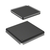
HD6417727F100CV Renesas Electronics America, HD6417727F100CV Datasheet - Page 695

HD6417727F100CV
Manufacturer Part Number
HD6417727F100CV
Description
SH3-DSP, LEAD FREE
Manufacturer
Renesas Electronics America
Series
SuperH® SH7700r
Datasheet
1.HD6417727BP100CV.pdf
(1098 pages)
Specifications of HD6417727F100CV
Core Processor
SH-3 DSP
Core Size
32-Bit
Speed
100MHz
Connectivity
FIFO, SCI, SIO, SmartCard, USB
Peripherals
DMA, LCD, POR, WDT
Number Of I /o
104
Program Memory Type
ROMless
Ram Size
32K x 8
Voltage - Supply (vcc/vdd)
1.6 V ~ 2.05 V
Data Converters
A/D 6x10b; D/A 2x8b
Oscillator Type
Internal
Operating Temperature
-20°C ~ 75°C
Package / Case
240-QFP Exposed Pad, 240-eQFP, 240-HQFP
Cpu Family
SuperH
Device Core Size
32b
Frequency (max)
100MHz
Interface Type
SCI/USB
Program Memory Size
Not Required
Total Internal Ram Size
16KB
# I/os (max)
104
Number Of Timers - General Purpose
4
Operating Supply Voltage (typ)
1.8/3.3V
Operating Supply Voltage (max)
2.05/3.6V
Operating Supply Voltage (min)
1.6/2.6V
On-chip Adc
6-chx10-bit
On-chip Dac
2-chx8-bit
Instruction Set Architecture
RISC
Operating Temp Range
-20C to 75C
Operating Temperature Classification
Commercial
Mounting
Surface Mount
Pin Count
240
Package Type
HQFP
Lead Free Status / RoHS Status
Lead free / RoHS Compliant
Eeprom Size
-
Program Memory Size
-
Lead Free Status / Rohs Status
Compliant
- Current page: 695 of 1098
- Download datasheet (7Mb)
20.3.5
Control data outputs the control command to CODEC and receive the state of CODEC. SIOF
support the following two operations as an interface operation of control data.
• Control by the slot positions
• Control by secondary FS
Control data is effective when selecting 16 bit as data length and MSB first receive mode.
(1) Control by Slot Positions (Master Mode 1)
This is the method that dedicates the slot passion of control data in a frame to transmit or receive
the control data.
Figure 20.7 shows a sample of control data interface timing by slot position.
Note: When using this method, peripheral clock (Pφ) should be used as the master clock (Master
SCK_SIO
SIOFSYNC
TXD_SIO
RXD_SIO
Clock Select (MSSEL) = 1).
Control Data Interface
Setting: TRMD = 00 or 10, REDG = 0,
TDLE = 1,
RDLE = 1,
CD0E = 1,
Slot No.0 Slot No.1 Slot No.2 Slot No.3
Lch. DATA Control ch.0 Rch. DATA Control ch.1
Figure 20.7 Control Data Interface (Slot Position)
TDLA3 to TDLA0 = 0000,
RDLA3 to RDLA0 = 0000,
CD0A3 to CD0A0 = 0001,
1 frame
Rev.6.00 Mar. 27, 2009 Page 637 of 1036
FL = (frame length 128 bits),
TDRE = 1,
RDRE = 1,
CD1E = 1,
—
Section 20 Serial IO (SIOF)
TDRA3 to TDRA0 = 0010,
RDRA3 to RDRA0 = 0010,
CD1A3 to CD1A0 = 0011
REJ09B0254-0600
Related parts for HD6417727F100CV
Image
Part Number
Description
Manufacturer
Datasheet
Request
R

Part Number:
Description:
KIT STARTER FOR M16C/29
Manufacturer:
Renesas Electronics America
Datasheet:

Part Number:
Description:
KIT STARTER FOR R8C/2D
Manufacturer:
Renesas Electronics America
Datasheet:

Part Number:
Description:
R0K33062P STARTER KIT
Manufacturer:
Renesas Electronics America
Datasheet:

Part Number:
Description:
KIT STARTER FOR R8C/23 E8A
Manufacturer:
Renesas Electronics America
Datasheet:

Part Number:
Description:
KIT STARTER FOR R8C/25
Manufacturer:
Renesas Electronics America
Datasheet:

Part Number:
Description:
KIT STARTER H8S2456 SHARPE DSPLY
Manufacturer:
Renesas Electronics America
Datasheet:

Part Number:
Description:
KIT STARTER FOR R8C38C
Manufacturer:
Renesas Electronics America
Datasheet:

Part Number:
Description:
KIT STARTER FOR R8C35C
Manufacturer:
Renesas Electronics America
Datasheet:

Part Number:
Description:
KIT STARTER FOR R8CL3AC+LCD APPS
Manufacturer:
Renesas Electronics America
Datasheet:

Part Number:
Description:
KIT STARTER FOR RX610
Manufacturer:
Renesas Electronics America
Datasheet:

Part Number:
Description:
KIT STARTER FOR R32C/118
Manufacturer:
Renesas Electronics America
Datasheet:

Part Number:
Description:
KIT DEV RSK-R8C/26-29
Manufacturer:
Renesas Electronics America
Datasheet:

Part Number:
Description:
KIT STARTER FOR SH7124
Manufacturer:
Renesas Electronics America
Datasheet:

Part Number:
Description:
KIT STARTER FOR H8SX/1622
Manufacturer:
Renesas Electronics America
Datasheet:

Part Number:
Description:
KIT DEV FOR SH7203
Manufacturer:
Renesas Electronics America
Datasheet:


