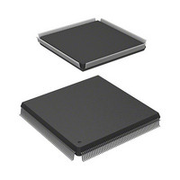
HD6417727F100CV Renesas Electronics America, HD6417727F100CV Datasheet - Page 441

HD6417727F100CV
Manufacturer Part Number
HD6417727F100CV
Description
SH3-DSP, LEAD FREE
Manufacturer
Renesas Electronics America
Series
SuperH® SH7700r
Datasheet
1.HD6417727BP100CV.pdf
(1098 pages)
Specifications of HD6417727F100CV
Core Processor
SH-3 DSP
Core Size
32-Bit
Speed
100MHz
Connectivity
FIFO, SCI, SIO, SmartCard, USB
Peripherals
DMA, LCD, POR, WDT
Number Of I /o
104
Program Memory Type
ROMless
Ram Size
32K x 8
Voltage - Supply (vcc/vdd)
1.6 V ~ 2.05 V
Data Converters
A/D 6x10b; D/A 2x8b
Oscillator Type
Internal
Operating Temperature
-20°C ~ 75°C
Package / Case
240-QFP Exposed Pad, 240-eQFP, 240-HQFP
Cpu Family
SuperH
Device Core Size
32b
Frequency (max)
100MHz
Interface Type
SCI/USB
Program Memory Size
Not Required
Total Internal Ram Size
16KB
# I/os (max)
104
Number Of Timers - General Purpose
4
Operating Supply Voltage (typ)
1.8/3.3V
Operating Supply Voltage (max)
2.05/3.6V
Operating Supply Voltage (min)
1.6/2.6V
On-chip Adc
6-chx10-bit
On-chip Dac
2-chx8-bit
Instruction Set Architecture
RISC
Operating Temp Range
-20C to 75C
Operating Temperature Classification
Commercial
Mounting
Surface Mount
Pin Count
240
Package Type
HQFP
Lead Free Status / RoHS Status
Lead free / RoHS Compliant
Eeprom Size
-
Program Memory Size
-
Lead Free Status / Rohs Status
Compliant
- Current page: 441 of 1098
- Download datasheet (7Mb)
Channel
2
3
Shared
Notes: These registers are located in area 1 of physical space. Therefore, when the cache is on,
either access these registers from the P2 area of logical space or else make an appropriate
setting using the MMU so that these registers are not cached.
1. Only a write of 0 after a read of 1 to clear a flag is enabled for bit 1 in CHCR0 to
2. If SAR0 to SAR3, DAR0 to DAR3, and CHCR0 to CHCR3 are accessed in 16 bits, the
3. DMATCR comprises the 24 bits from bit 0 to bit 23. The upper 8 bits, bits 24 to 31,
4. When address translation by the MMU does not apply, the address in parentheses
Name
DMA source address
register 2
DMA destination address
register 2
DMA transfer count
register 2
DMA channel control
register 2
DMA source address
register 3
DMA destination address
register 3
DMA transfer count
register 3
DMA channel control
register 3
DMA operation register
DMA channel assign
register
CHCR3 and bits 1 and 2 in DMAOR.
16 bit values that were not accessed are held.
cannot be written with 1 and are always read as 0.
should be used.
Abbrevi-
ation
SAR2
DAR2
DMATCR2 R/W
CHCR2
SAR3
DAR3
DMATCR3 R/W
CHCR3
DMAOR
CHRAR
Section 14 Direct Memory Access Controller (DMAC)
R/W
R/W
R/W
R/W *
R/W
R/W
R/W *
R/W *
R/W
1
1
1
Initial
Value
Undefined
Undefined
Undefined
H'00000000 H'0400004C
Undefined
Undefined
Undefined
H'00000000 H'0400005C
H'0000
H’0000
Rev.6.00 Mar. 27, 2009 Page 383 of 1036
Address
H'04000040
(H'A4000040) *
H'04000044
(H'A4000044) *
H'04000048
(H'A4000048) *
(H'A400004C) *
H'04000050
(H'A4000050) *
H'04000054
(H'A4000054) *
H'04000058
(H'A4000058) *
(H'A400005C) *
H'04000060
(H'A4000060) *
H’0400022A
(H’A400022A) *
4
4
4
4
4
4
4
4
4
4
REJ09B0254-0600
Register
Size
32 bits
32 bits
24 bits
32 bits
32 bits
32 bits
24 bits
32 bits
16 bits
16 bits
Access
Size
16, 32 *
16, 32 *
16, 32 *
8, 16, 32 *
16, 32 *
16, 32 *
16, 32 *
8, 16, 32 *
8, 16 *
16
2
2
2
3
2
2
3
2
2
Related parts for HD6417727F100CV
Image
Part Number
Description
Manufacturer
Datasheet
Request
R

Part Number:
Description:
KIT STARTER FOR M16C/29
Manufacturer:
Renesas Electronics America
Datasheet:

Part Number:
Description:
KIT STARTER FOR R8C/2D
Manufacturer:
Renesas Electronics America
Datasheet:

Part Number:
Description:
R0K33062P STARTER KIT
Manufacturer:
Renesas Electronics America
Datasheet:

Part Number:
Description:
KIT STARTER FOR R8C/23 E8A
Manufacturer:
Renesas Electronics America
Datasheet:

Part Number:
Description:
KIT STARTER FOR R8C/25
Manufacturer:
Renesas Electronics America
Datasheet:

Part Number:
Description:
KIT STARTER H8S2456 SHARPE DSPLY
Manufacturer:
Renesas Electronics America
Datasheet:

Part Number:
Description:
KIT STARTER FOR R8C38C
Manufacturer:
Renesas Electronics America
Datasheet:

Part Number:
Description:
KIT STARTER FOR R8C35C
Manufacturer:
Renesas Electronics America
Datasheet:

Part Number:
Description:
KIT STARTER FOR R8CL3AC+LCD APPS
Manufacturer:
Renesas Electronics America
Datasheet:

Part Number:
Description:
KIT STARTER FOR RX610
Manufacturer:
Renesas Electronics America
Datasheet:

Part Number:
Description:
KIT STARTER FOR R32C/118
Manufacturer:
Renesas Electronics America
Datasheet:

Part Number:
Description:
KIT DEV RSK-R8C/26-29
Manufacturer:
Renesas Electronics America
Datasheet:

Part Number:
Description:
KIT STARTER FOR SH7124
Manufacturer:
Renesas Electronics America
Datasheet:

Part Number:
Description:
KIT STARTER FOR H8SX/1622
Manufacturer:
Renesas Electronics America
Datasheet:

Part Number:
Description:
KIT DEV FOR SH7203
Manufacturer:
Renesas Electronics America
Datasheet:


