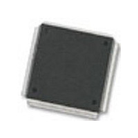
MC68376BAMFT20 Freescale Semiconductor, MC68376BAMFT20 Datasheet - Page 100

MC68376BAMFT20
Manufacturer Part Number
MC68376BAMFT20
Description
Manufacturer
Freescale Semiconductor
Datasheet
1.MC68376BAMFT20.pdf
(434 pages)
Specifications of MC68376BAMFT20
Cpu Family
68K/M683xx
Device Core
ColdFire
Device Core Size
32b
Frequency (max)
20MHz
Interface Type
QSPI/SCI
Program Memory Type
ROM
Program Memory Size
8KB
Total Internal Ram Size
7.5KB
# I/os (max)
18
Number Of Timers - General Purpose
2
Operating Supply Voltage (typ)
5V
Operating Supply Voltage (max)
5.25V
Operating Supply Voltage (min)
4.75V
On-chip Adc
16-chx10-bit
Instruction Set Architecture
RISC
Operating Temp Range
-40C to 125C
Operating Temperature Classification
Automotive
Mounting
Surface Mount
Pin Count
160
Package Type
PQFP
Lead Free Status / Rohs Status
Not Compliant
Available stocks
Company
Part Number
Manufacturer
Quantity
Price
Company:
Part Number:
MC68376BAMFT20
Manufacturer:
FREESCAL
Quantity:
245
- Current page: 100 of 434
- Download datasheet (7Mb)
5.5.1.4 Data Strobe
5.5.1.5 Read/Write Signal
5.5.1.6 Size Signals
5.5.1.7 Function Codes
5-22
MOTOROLA
Data strobe (DS) is a timing signal. For a read cycle, the MCU asserts DS to signal an
external device to place data on the bus. DS is asserted at the same time as AS during
a read cycle. For a write cycle, DS signals an external device that data on the bus is
valid. The MCU asserts DS one full clock cycle after the assertion of AS during a write
cycle.
The read/write signal (R/W) determines the direction of the transfer during a bus cycle.
This signal changes state, when required, at the beginning of a bus cycle, and is valid
while AS is asserted. R/W only transitions when a write cycle is preceded by a read
cycle or vice versa. The signal may remain low for two consecutive write cycles.
Size signals (SIZ[1:0]) indicate the number of bytes remaining to be transferred during
an operand cycle. They are valid while the AS is asserted. Table 5-9 shows SIZ0 and
SIZ1 encoding.
The CPU generates function code signals (FC[2:0]) to indicate the type of activity oc-
curring on the data or address bus. These signals can be considered address exten-
sions that can be externally decoded to determine which of eight external address
spaces is accessed during a bus cycle.
Address space 7 is designated CPU space. CPU space is used for control information
not normally associated with read or write bus cycles. Function codes are valid while
AS is asserted.
Table 5-10 shows address space encoding.
Table 5-9 Size Signal Encoding
SIZ1
0
1
1
0
SYSTEM INTEGRATION MODULE
SIZ0
1
0
1
0
Transfer Size
Three bytes
Long word
Word
Byte
USER’S MANUAL
MC68336/376
Related parts for MC68376BAMFT20
Image
Part Number
Description
Manufacturer
Datasheet
Request
R
Part Number:
Description:
Manufacturer:
Freescale Semiconductor, Inc
Datasheet:
Part Number:
Description:
Manufacturer:
Freescale Semiconductor, Inc
Datasheet:
Part Number:
Description:
Manufacturer:
Freescale Semiconductor, Inc
Datasheet:
Part Number:
Description:
Manufacturer:
Freescale Semiconductor, Inc
Datasheet:
Part Number:
Description:
Manufacturer:
Freescale Semiconductor, Inc
Datasheet:
Part Number:
Description:
Manufacturer:
Freescale Semiconductor, Inc
Datasheet:
Part Number:
Description:
Manufacturer:
Freescale Semiconductor, Inc
Datasheet:
Part Number:
Description:
Manufacturer:
Freescale Semiconductor, Inc
Datasheet:
Part Number:
Description:
Manufacturer:
Freescale Semiconductor, Inc
Datasheet:
Part Number:
Description:
Manufacturer:
Freescale Semiconductor, Inc
Datasheet:
Part Number:
Description:
Manufacturer:
Freescale Semiconductor, Inc
Datasheet:
Part Number:
Description:
Manufacturer:
Freescale Semiconductor, Inc
Datasheet:
Part Number:
Description:
Manufacturer:
Freescale Semiconductor, Inc
Datasheet:
Part Number:
Description:
Manufacturer:
Freescale Semiconductor, Inc
Datasheet:
Part Number:
Description:
Manufacturer:
Freescale Semiconductor, Inc
Datasheet:


