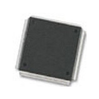
MC68376BAMFT20 Freescale Semiconductor, MC68376BAMFT20 Datasheet - Page 171

MC68376BAMFT20
Manufacturer Part Number
MC68376BAMFT20
Description
Manufacturer
Freescale Semiconductor
Datasheet
1.MC68376BAMFT20.pdf
(434 pages)
Specifications of MC68376BAMFT20
Cpu Family
68K/M683xx
Device Core
ColdFire
Device Core Size
32b
Frequency (max)
20MHz
Interface Type
QSPI/SCI
Program Memory Type
ROM
Program Memory Size
8KB
Total Internal Ram Size
7.5KB
# I/os (max)
18
Number Of Timers - General Purpose
2
Operating Supply Voltage (typ)
5V
Operating Supply Voltage (max)
5.25V
Operating Supply Voltage (min)
4.75V
On-chip Adc
16-chx10-bit
Instruction Set Architecture
RISC
Operating Temp Range
-40C to 125C
Operating Temperature Classification
Automotive
Mounting
Surface Mount
Pin Count
160
Package Type
PQFP
Lead Free Status / Rohs Status
Not Compliant
Available stocks
Company
Part Number
Manufacturer
Quantity
Price
Company:
Part Number:
MC68376BAMFT20
Manufacturer:
FREESCAL
Quantity:
245
- Current page: 171 of 434
- Download datasheet (7Mb)
9.4 Serial Communication Interface
9.4.1 SCI Registers
9.4.1.1 Control Registers
MC68336/376
USER’S MANUAL
To configure a peripheral chip-select, set the appropriate bit in PQSPAR, then config-
ure the chip-select pin as an output by setting the appropriate bit in DDRQS. The value
of the bit in PORTQS that corresponds to the chip-select pin determines the base state
of the chip-select signal. If base state is zero, chip-select assertion must be active high
(PCS bit in command RAM must be set); if base state is one, assertion must be active
low (PCS bit in command RAM must be cleared). PORTQS bits are cleared during re-
set. If no new data is written to PORTQS before pin assignment and configuration as
an output, base state of chip-select signals is zero and chip-select pins are configured
for active-high operation.
The serial communication interface (SCI) communicates with external devices through
an asynchronous serial bus. The SCI uses a standard non-return to zero (NRZ) trans-
mission format. The SCI is fully compatible with other Motorola SCI systems, such as
those on M68HC11 and M68HC05 devices. Figure 9-10 is a block diagram of the SCI
transmitter. Figure 9-11 is a block diagram of the SCI receiver.
The SCI programming model includes the QSM global and pin control registers, and
four SCI registers. There are two SCI control registers (SCCR0 and SCCR1), one sta-
tus register (SCSR), and one data register (SCDR). Refer to D.6 Queued Serial Mod-
ule for register bit and field definitions.
SCCR0 contains the baud rate selection field. Baud rate must be set before the SCI is
enabled. This register can be read or written.
SCCR1 contains a number of SCI configuration parameters, including transmitter and
receiver enable bits, interrupt enable bits, and operating mode enable bits. This regis-
ter can be read or written at any time. The SCI can modify the RWU bit under certain
circumstances.
Changing the value of SCI control bits during a transfer may disrupt operation. Before
changing register values, allow the SCI to complete the current transfer, then disable
the receiver and transmitter.
QUEUED SERIAL MODULE
MOTOROLA
9-21
Related parts for MC68376BAMFT20
Image
Part Number
Description
Manufacturer
Datasheet
Request
R
Part Number:
Description:
Manufacturer:
Freescale Semiconductor, Inc
Datasheet:
Part Number:
Description:
Manufacturer:
Freescale Semiconductor, Inc
Datasheet:
Part Number:
Description:
Manufacturer:
Freescale Semiconductor, Inc
Datasheet:
Part Number:
Description:
Manufacturer:
Freescale Semiconductor, Inc
Datasheet:
Part Number:
Description:
Manufacturer:
Freescale Semiconductor, Inc
Datasheet:
Part Number:
Description:
Manufacturer:
Freescale Semiconductor, Inc
Datasheet:
Part Number:
Description:
Manufacturer:
Freescale Semiconductor, Inc
Datasheet:
Part Number:
Description:
Manufacturer:
Freescale Semiconductor, Inc
Datasheet:
Part Number:
Description:
Manufacturer:
Freescale Semiconductor, Inc
Datasheet:
Part Number:
Description:
Manufacturer:
Freescale Semiconductor, Inc
Datasheet:
Part Number:
Description:
Manufacturer:
Freescale Semiconductor, Inc
Datasheet:
Part Number:
Description:
Manufacturer:
Freescale Semiconductor, Inc
Datasheet:
Part Number:
Description:
Manufacturer:
Freescale Semiconductor, Inc
Datasheet:
Part Number:
Description:
Manufacturer:
Freescale Semiconductor, Inc
Datasheet:
Part Number:
Description:
Manufacturer:
Freescale Semiconductor, Inc
Datasheet:


