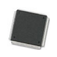
MC68376BAMFT20 Freescale Semiconductor, MC68376BAMFT20 Datasheet - Page 147

MC68376BAMFT20
Manufacturer Part Number
MC68376BAMFT20
Description
Manufacturer
Freescale Semiconductor
Datasheet
1.MC68376BAMFT20.pdf
(434 pages)
Specifications of MC68376BAMFT20
Cpu Family
68K/M683xx
Device Core
ColdFire
Device Core Size
32b
Frequency (max)
20MHz
Interface Type
QSPI/SCI
Program Memory Type
ROM
Program Memory Size
8KB
Total Internal Ram Size
7.5KB
# I/os (max)
18
Number Of Timers - General Purpose
2
Operating Supply Voltage (typ)
5V
Operating Supply Voltage (max)
5.25V
Operating Supply Voltage (min)
4.75V
On-chip Adc
16-chx10-bit
Instruction Set Architecture
RISC
Operating Temp Range
-40C to 125C
Operating Temperature Classification
Automotive
Mounting
Surface Mount
Pin Count
160
Package Type
PQFP
Lead Free Status / Rohs Status
Not Compliant
Available stocks
Company
Part Number
Manufacturer
Quantity
Price
Company:
Part Number:
MC68376BAMFT20
Manufacturer:
FREESCAL
Quantity:
245
- Current page: 147 of 434
- Download datasheet (7Mb)
7.1 MRM Register Block
7.2 MRM Array Address Mapping
MC68336/376
USER’S MANUAL
The masked ROM module (MRM) consists of a fixed-location control register block
and an 8-Kbyte mask-programmed read-only memory array that can be mapped to
any 8-Kbyte boundary in the system memory map. The MRM can be programmed to
insert wait states to accommodate migration from slow external development memory.
Access time depends upon the number of wait states specified, but can be as fast as
two bus cycles. The MRM can be used for program accesses only, or for program and
data accesses. Data can be read in bytes, words or long words. The MRM can be con-
figured to support system bootstrap during reset.
There are three MRM control registers: the masked ROM module configuration regis-
ter (MRMCR), and the ROM array base address registers (ROMBAH and ROMBAL).
In addition, the MRM register block contains signature registers (SIGHI and SIGLO),
and ROM bootstrap words (ROMBS[0:3]).
The module mapping bit (MM) in the SIM configuration register defines the most
significant bit (ADDR23) of the IMB address for each MC68336/376 module. 5.2.1
Module Mapping contains information about how the state of MM affects the system.
The MRM control register block consists of 32 bytes, but not all locations are imple-
mented. Unimplemented register addresses are read as zeros, and writes have no ef-
fect. Refer to D.4 Masked ROM Module for register block address map and register
bit/field definitions.
Base address registers ROMBAH and ROMBAL are used to specify the ROM array
base address in the memory map. Although the base address contained in ROMBAH
and ROMBAL is mask-programmed, these registers can be written after reset to
change the default array address if the base address lock bit (LOCK in MRMCR) is not
masked to a value of one.
The MRM array can be mapped to any 8-Kbyte boundary in the memory map, but must
not overlap other module control registers (overlap makes the registers inaccessible).
If the array overlaps the MRM register block, addresses in the block are accessed in-
stead of the corresponding array addresses.
ROMBAH and ROMBAL can only be written while the ROM is in low-power stop mode
(MRMCR STOP = 1) and the base address lock (MRMCR LOCK = 0) is disabled.
LOCK can be written once only to a value of one. This prevents accidental remapping
of the array.
SECTION 7 MASKED ROM MODULE
MASKED ROM MODULE
MOTOROLA
7-1
Related parts for MC68376BAMFT20
Image
Part Number
Description
Manufacturer
Datasheet
Request
R
Part Number:
Description:
Manufacturer:
Freescale Semiconductor, Inc
Datasheet:
Part Number:
Description:
Manufacturer:
Freescale Semiconductor, Inc
Datasheet:
Part Number:
Description:
Manufacturer:
Freescale Semiconductor, Inc
Datasheet:
Part Number:
Description:
Manufacturer:
Freescale Semiconductor, Inc
Datasheet:
Part Number:
Description:
Manufacturer:
Freescale Semiconductor, Inc
Datasheet:
Part Number:
Description:
Manufacturer:
Freescale Semiconductor, Inc
Datasheet:
Part Number:
Description:
Manufacturer:
Freescale Semiconductor, Inc
Datasheet:
Part Number:
Description:
Manufacturer:
Freescale Semiconductor, Inc
Datasheet:
Part Number:
Description:
Manufacturer:
Freescale Semiconductor, Inc
Datasheet:
Part Number:
Description:
Manufacturer:
Freescale Semiconductor, Inc
Datasheet:
Part Number:
Description:
Manufacturer:
Freescale Semiconductor, Inc
Datasheet:
Part Number:
Description:
Manufacturer:
Freescale Semiconductor, Inc
Datasheet:
Part Number:
Description:
Manufacturer:
Freescale Semiconductor, Inc
Datasheet:
Part Number:
Description:
Manufacturer:
Freescale Semiconductor, Inc
Datasheet:
Part Number:
Description:
Manufacturer:
Freescale Semiconductor, Inc
Datasheet:


