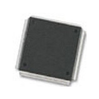
MC68376BAMFT20 Freescale Semiconductor, MC68376BAMFT20 Datasheet - Page 53

MC68376BAMFT20
Manufacturer Part Number
MC68376BAMFT20
Description
Manufacturer
Freescale Semiconductor
Datasheet
1.MC68376BAMFT20.pdf
(434 pages)
Specifications of MC68376BAMFT20
Cpu Family
68K/M683xx
Device Core
ColdFire
Device Core Size
32b
Frequency (max)
20MHz
Interface Type
QSPI/SCI
Program Memory Type
ROM
Program Memory Size
8KB
Total Internal Ram Size
7.5KB
# I/os (max)
18
Number Of Timers - General Purpose
2
Operating Supply Voltage (typ)
5V
Operating Supply Voltage (max)
5.25V
Operating Supply Voltage (min)
4.75V
On-chip Adc
16-chx10-bit
Instruction Set Architecture
RISC
Operating Temp Range
-40C to 125C
Operating Temperature Classification
Automotive
Mounting
Surface Mount
Pin Count
160
Package Type
PQFP
Lead Free Status / Rohs Status
Not Compliant
Available stocks
Company
Part Number
Manufacturer
Quantity
Price
Company:
Part Number:
MC68376BAMFT20
Manufacturer:
FREESCAL
Quantity:
245
- Current page: 53 of 434
- Download datasheet (7Mb)
4.1 General
MC68336/376
USER’S MANUAL
The CPU32, the instruction processing module of the M68300 family, is based on the
industry-standard MC68000 processor. It has many features of the MC68010 and
MC68020, as well as unique features suited for high-performance controller applica-
tions. This section is an overview of the CPU32. For detailed information concerning
CPU operation, refer to the CPU32 Reference Manual (CPU32RM/AD).
Ease of programming is an important consideration in using a microcontroller. The
CPU32 instruction format reflects a philosophy emphasizing register-memory interac-
tion. There are eight multifunction data registers and seven general-purpose address-
ing registers.
All data resources are available to all operations requiring those resources. The data
registers readily support 8-bit (byte), 16-bit (word), and 32-bit (long-word) operand
lengths for all operations. Word and long-word operations support address manipula-
tion. Although the program counter (PC) and stack pointers (SP) are special-purpose
registers, they are also available for most data addressing activities. Ease of program
checking and diagnosis is further enhanced by trace and trap capabilities at the in-
struction level.
A block diagram of the CPU32 is shown in Figure 4-1. The major blocks operate in a
highly independent fashion that maximizes concurrency of operation while managing
the essential synchronization of instruction execution and bus operation. The bus con-
troller loads instructions from the data bus into the decode unit. The sequencer and
control unit provide overall chip control, managing the internal buses, registers, and
functions of the execution unit.
SECTION 4 CENTRAL PROCESSOR UNIT
CENTRAL PROCESSOR UNIT
MOTOROLA
4-1
Related parts for MC68376BAMFT20
Image
Part Number
Description
Manufacturer
Datasheet
Request
R
Part Number:
Description:
Manufacturer:
Freescale Semiconductor, Inc
Datasheet:
Part Number:
Description:
Manufacturer:
Freescale Semiconductor, Inc
Datasheet:
Part Number:
Description:
Manufacturer:
Freescale Semiconductor, Inc
Datasheet:
Part Number:
Description:
Manufacturer:
Freescale Semiconductor, Inc
Datasheet:
Part Number:
Description:
Manufacturer:
Freescale Semiconductor, Inc
Datasheet:
Part Number:
Description:
Manufacturer:
Freescale Semiconductor, Inc
Datasheet:
Part Number:
Description:
Manufacturer:
Freescale Semiconductor, Inc
Datasheet:
Part Number:
Description:
Manufacturer:
Freescale Semiconductor, Inc
Datasheet:
Part Number:
Description:
Manufacturer:
Freescale Semiconductor, Inc
Datasheet:
Part Number:
Description:
Manufacturer:
Freescale Semiconductor, Inc
Datasheet:
Part Number:
Description:
Manufacturer:
Freescale Semiconductor, Inc
Datasheet:
Part Number:
Description:
Manufacturer:
Freescale Semiconductor, Inc
Datasheet:
Part Number:
Description:
Manufacturer:
Freescale Semiconductor, Inc
Datasheet:
Part Number:
Description:
Manufacturer:
Freescale Semiconductor, Inc
Datasheet:
Part Number:
Description:
Manufacturer:
Freescale Semiconductor, Inc
Datasheet:


