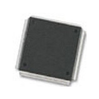
MC68376BAMFT20 Freescale Semiconductor, MC68376BAMFT20 Datasheet - Page 99

MC68376BAMFT20
Manufacturer Part Number
MC68376BAMFT20
Description
Manufacturer
Freescale Semiconductor
Datasheet
1.MC68376BAMFT20.pdf
(434 pages)
Specifications of MC68376BAMFT20
Cpu Family
68K/M683xx
Device Core
ColdFire
Device Core Size
32b
Frequency (max)
20MHz
Interface Type
QSPI/SCI
Program Memory Type
ROM
Program Memory Size
8KB
Total Internal Ram Size
7.5KB
# I/os (max)
18
Number Of Timers - General Purpose
2
Operating Supply Voltage (typ)
5V
Operating Supply Voltage (max)
5.25V
Operating Supply Voltage (min)
4.75V
On-chip Adc
16-chx10-bit
Instruction Set Architecture
RISC
Operating Temp Range
-40C to 125C
Operating Temperature Classification
Automotive
Mounting
Surface Mount
Pin Count
160
Package Type
PQFP
Lead Free Status / Rohs Status
Not Compliant
Available stocks
Company
Part Number
Manufacturer
Quantity
Price
Company:
Part Number:
MC68376BAMFT20
Manufacturer:
FREESCAL
Quantity:
245
- Current page: 99 of 434
- Download datasheet (7Mb)
5.5.1 Bus Control Signals
5.5.1.1 Address Bus
5.5.1.2 Address Strobe
5.5.1.3 Data Bus
MC68336/376
USER’S MANUAL
The external bus has 24 address lines and 16 data lines. The EBI provides dynamic
sizing between 8-bit and 16-bit data accesses. It supports byte, word, and long-word
transfers. Port width is the maximum number of bits accepted or provided during a bus
transfer. Widths of eight and sixteen bits are accessed through the use of asynchro-
nous cycles controlled by the size (SIZ1 and SIZ0) and data and size acknowledge
(DSACK1 and DSACK0) pins. Multiple bus cycles may be required for dynamically
sized transfers.
To add flexibility and minimize the necessity for external logic, MCU chip-select logic
can be synchronized with EBI transfers. Refer to 5.9 Chip-Selects for more informa-
tion.
The address bus provides addressing information to external devices. The data bus
transfers 8-bit and 16-bit data between the MCU and external devices. Strobe signals,
one for the address bus and another for the data bus, indicate the validity of an ad-
dress and provide timing information for data.
Control signals indicate the beginning of each bus cycle, the address space it is to take
place in, the size of the transfer, and the type of cycle. External devices decode these
signals and respond to transfer data and terminate the bus cycle. The EBI operates in
an asynchronous mode for any port width.
Bus signals ADDR[23:0] define the address of the byte (or the most significant byte)
to be transferred during a bus cycle. The MCU places the address on the bus at the
beginning of a bus cycle. The address is valid while AS is asserted.
Address strobe (AS) is a timing signal that indicates the validity of an address on the
address bus and of many control signals. It is asserted one-half clock after the begin-
ning of a bus cycle.
Signals DATA[15:0] form a bidirectional, non-multiplexed parallel bus that transfers
data to or from the MCU. A read or write operation can transfer eight or sixteen bits of
data in one bus cycle. During a read cycle, the data is latched by the MCU on the last
falling edge of the clock for that bus cycle. For a write cycle, all 16 bits of the data bus
are driven, regardless of the port width or operand size. The MCU places the data on
the data bus one-half clock cycle after AS is asserted in a write cycle.
SYSTEM INTEGRATION MODULE
MOTOROLA
5-21
Related parts for MC68376BAMFT20
Image
Part Number
Description
Manufacturer
Datasheet
Request
R
Part Number:
Description:
Manufacturer:
Freescale Semiconductor, Inc
Datasheet:
Part Number:
Description:
Manufacturer:
Freescale Semiconductor, Inc
Datasheet:
Part Number:
Description:
Manufacturer:
Freescale Semiconductor, Inc
Datasheet:
Part Number:
Description:
Manufacturer:
Freescale Semiconductor, Inc
Datasheet:
Part Number:
Description:
Manufacturer:
Freescale Semiconductor, Inc
Datasheet:
Part Number:
Description:
Manufacturer:
Freescale Semiconductor, Inc
Datasheet:
Part Number:
Description:
Manufacturer:
Freescale Semiconductor, Inc
Datasheet:
Part Number:
Description:
Manufacturer:
Freescale Semiconductor, Inc
Datasheet:
Part Number:
Description:
Manufacturer:
Freescale Semiconductor, Inc
Datasheet:
Part Number:
Description:
Manufacturer:
Freescale Semiconductor, Inc
Datasheet:
Part Number:
Description:
Manufacturer:
Freescale Semiconductor, Inc
Datasheet:
Part Number:
Description:
Manufacturer:
Freescale Semiconductor, Inc
Datasheet:
Part Number:
Description:
Manufacturer:
Freescale Semiconductor, Inc
Datasheet:
Part Number:
Description:
Manufacturer:
Freescale Semiconductor, Inc
Datasheet:
Part Number:
Description:
Manufacturer:
Freescale Semiconductor, Inc
Datasheet:


